Single Pentode Wien Bridge Oscillator
Single Pentode Wien Bridge Oscillator

Fellow Radiophiles:
William Hewlett, co-founder of Hewlett-Packard, pioneered the use of the Wien Bridge oscillator with his 1939 Electrical Engineering Master's thesis at Stanford University. His oscillator sought to use resistors and capacitors instead of bulky low frequency LC tank circuits to generate audio frequencies. He obtained low distortion (<0.5%) with the use of a two stage amplifier with enough negative feedback to set it's gain to just 3, as required for oscillation of the Wien Bridge circuit. He used a light bulb to serve as amplitude detector and linear gain setting resistor for the fed-back amplifier. Hewlett credits L. A. Meacham with the use of the light bulb for automatic oscillator gain stabilization as published in the Bell System Technical Journal Vol 17, p. 574, 0ctober 1938.

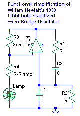 The Wien Bridge network was invented by Max Wien in 1891. This excerpt from Hewlett's thesis shows half the bridge. At the resonant frequency with equal resistors and capacitors, the attenuation is 1/3 of the input voltage with zero phase shift. This means that if an exact gain of 3 can be provided from the output of the network to the input, we have a sinusoidal oscillator.
Hewlett's original 1939 oscillator circuit is shown below the resonance curves.
The simplified circuit on the right shows the lamp that stabilizes the non-inverting gain of the fed-back amplifier to exactly 3x. The lamp resistance increases when a larger signal is applied to it. This means that if oscillations grow too large, the lamp resistance increases to reduce oscillation 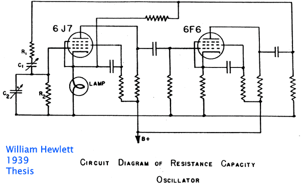 amplitude until a stable equilibrium is reached. At this equilibrium point, the RC-CR Wien network forces a gain of 3x at the fed-back amplifier, which is to say, it forces the lamp resistance to a value that yields an amplifier gain of 3x. In turn, the Lamp forces the Wien network oscillation amplitude.
This lamp stabilized Wien bridge oscillator differs fundamentally from RF LC oscillators commonly used in Radio circuits in that the oscillation currents and voltages in the Wien oscillator always remain nearly perfectly sinusoidal. Typical RF oscillators with an LC tank circuit have a very pure sine wave voltage across the the tank circuit, but the oscillations are stimulated with very non-linear current pulses in a class C regime. The high Q>100 of the LC tank circuit gives the Frequency of these RF oscillators a fair immunity from variations in the strength of the current pulses that stimulate the oscillations. The amplitude of these Class C RF oscillators is controlled by the self limitation of the current pulses or by localized AGC action on these current pulses.
As the plot above shows, the Wien bridge circuit has a very low Q. If a class C amplifier were used instead of the linear amplifier with a gain of 3, the oscillation frequency would be not only a function of the RC-CR network time constants, but also a function of the class C amplifier limiting characteristics. It is essential then that the gain-of-3 amplifier be a very linear amplifier to let the RC-CR network time constants be the sole determinants of the oscillation frequency.
One inconvenience of the Wien bridge oscillator is that it requires a non-inverting gain amplifier, which, in the tube era generally meant a cascade of two inverting stages. This often made the phase shift oscillator which requires an inverting gain, a good alternative for a single tube RC oscillator design. But Phase-shift oscillators require typically 4 or more RC pairs to obtain the 180o phase shift.
The Single Pentode Wien Bridge Oscillator
The non-inverting voltage gain that is possible between the suppressor grid G3 and the screen grid G2 in a dual control Pentode can be used to build a Wien Bridge oscillator with a single Pentode.
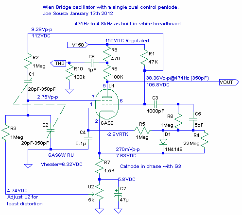
The following schematic shows the 6AS6 dual control pentode serving as the linear gain controlled amplifier with a gain of 3 from the suppressor grid G3 at pin 7 to the screen grid G2 at pin 6. The exact gain of 3 from G3 to G2 is controlled automatically with the DC bias at the control grid G1 at pin 1. In this particular implementation, the plate, which also amplifies signal from G3 feeds D1 1N4148 Silicon diode for detection via an AC-coupling RC network. The detected DC level at the diode becomes the AGC control voltage after filtering by R5 and C4 that is applied to the control grid G1. Note that the control voltage at G1 has negligible effect on the linearity of the G3-G2 transfer function. R8 and C1 serve to decouple the plate circuit from the non-linear loading of the 1N4148 AGC detection diode. Note that D1 has it's cathode tied to the cathode of the pentode. This means that a sharp cutoff pentode with dual control might have been constructed with an additional diode plate as was commonly done with some remote cutoff IF amplifier pentodes.
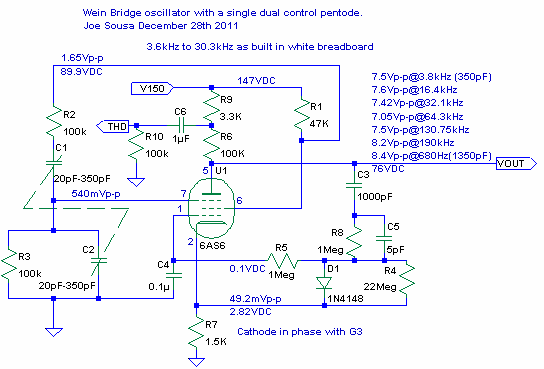
You may remember from the dual control Pentode discussion that the gain from G3 to the Plate is inverting, but this is of no concern for simple amplitude envelope detection by the diode. In this first implementation of the circuit, I chose to feed the detector circuit with the plate signal because the higher signal amplitude that was available at the plate forced the overall oscillation amplitude to lower levels for lower distortion. I was able to achieve 0.5% (-46dB) THD at 600Hz with R=100k and C=1350pF with this first circuit, after experimenting with various values of Plate and Screen G2 resistors for lowest distortion. I measured the distortion with the audio port in my PC.
One of the peculiar characteristics of the non-inverting gain from G3 to G2 is that adding a cathode resistor actually makes the gain from G3 to G2 go up. In other words, the cathode resistor causes G2-G3 gain regeneration, not degeneration, as is usually the case from G1 to the Plate with a cathode resistor. (Some of the peculiarities of G3 gain are explored in CK511X Reentrant Pentode Amplifier and in HI-FI AM transmitter).
Another important characteristic is the negative feedback that the Plate swing has on the swing at the screen grid G2. A plate load degenerates the gain from G3 to G2, but also makes this gain much more linear. This is the main reason why I have a resistive load at the plate.
Note that the schematic above shows that 540mVp-p at G3, causes 49.2mVp-p at the cathode in phase with G3. This cathode voltage is then amplified to the the screen grid G2 with the relatively strong G1-G2 transconductance. If the cathode is bypassed to ground with a large capacitor, the net gain from G3 to G2 is reduced.
The exact DC bias voltage at G3 is not terribly sensitive, so I simply grounded G3 via R3 and let the AGC controlled drop across the cathode resistor R7 also serve to bias G3 about -2.8V with respect to the cathode. Some negative bias is needed at G3 to prevent conduction.
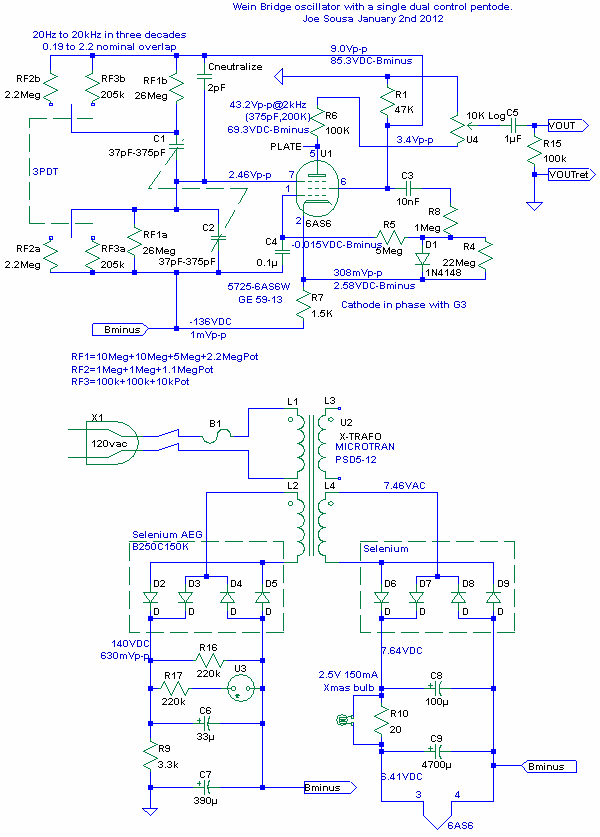
The following schematic shows the final version that I built into a permanent case.
Power supply
The power transformer is a common dual-primary transformer that is meant for operation at 110VAC or 220VAC, depending on parallel drive or serial drive to the primaries, respectively. My mains power is 110VAC, so I use the other primary as my isolated high voltage source. This means that the primary can only deliver half the current it could under normal shunt primary operation at 110VAC. This is OK because with only 34mArms drawn from the mains, I am drawing much less than half the full rated VA power.
The two secondaries are rated to deliver 6.3VAC under full load, but deliver 7.5V under the light 175mA load of the heater. The value of C8 is kept low for a low average DC voltage across it. R10 and the cute 2.5V 150mA light bulb serve to drop the 7.6VDC of the first cap to the 6.4V at the output cap. There is no hard necessity for the bulb, but I like to see it glow and turn on hard when the circuit is first powered up.
I chose to ground the positive end of the supply for lower hum at the output potentiometer at low levels. I also chose to drive the heater with DC to avoid stray hum injection into the circuit. This means that much of the circuitry that was grounded is now hot, including the big selenium rectifier. This forced me to add a protective cover to the power supply circuit. The neon bulb U3 across the high Votlage DC power supply serves to warn me that the large 390uF flash capacitor remains charged up for a while after the power is turned off until R16 eventually discharges it with an 85s time constant after several minutes.
Hum injection is most objectionable for oscillation frequencies near the 60Hz hum frequency and it's harmonics, because the very sensitive AGC circuit starts to amplitude modulate the oscillation amplitude at the hum/oscillator beat frequency. This sensitivity also forced me into a fully shielded enclosure. The DC heater supply gave me a great excuse to finally use the large NOS Selenium rectifier I have had for many years.
The Wien network sets the frequency
The current design has equal valued capacitors and resistors in the Wien network. Hewlett's thesis graph shown above has the oscillation frequency as 1/(2xPIxRxC) in Hertz. In the constructed version of the oscillator I added 3 selectable decade ranges to cover from 20Hz to 20kHz. A pair of permanently wired 26Meg resistors at RF1 set the lowest 20Hz-200Hz range. A 2P3T adds a pair of 2.2Meg resistors at RF2 in parallel with the first pair for the 200Hz-2kHz range, or a pair of 205k resistors at RF3 in parallel with the first pair for the 2kHz-20kHz range.
A dual 350pF variable capacitor with isolated shaft serves to tune the oscillator frequency continuously. I used an isolation nut on the capacitor shaft, but plastic knob with a plastic shaft that reached into the case would have worked too. I don't recommend bringing out the live shaft of the tuning cap with a plastic knob over it, because this will pick up hum.
Two 30pF trim capacitors across this variable cap limit each frequency range to one decade. Without this limitation the range was 50:1 with much of the range squeezed at the top end of cap rotation. The trim capacitor in parallel with C2 will be trimmed to a lower value than the trim capacitor in parallel with C1 because there is already some input capacitance at the suppressor grid G3. The ratio of C1 to C2 is adjusted with these trimmers to obtain the same output amplitude at the low end of the range as at the high end of the range. When the trimmers are set this way, the voltage signal at the output of the Wien circuit will always be 1/3 of the voltage signal at the top of the Wien circuit.
I added a quick crude neutralization 2pF capacitor from the Screen grid G2 at pin 6 to the Suppressor grid G3 at pin 7 to reduce input capacitance at the Suppressor grid G3.
Automatic Gain Control AGC
I moved the pick-off point for the AGC detector from the Plate shown in the first construction above to the screen grid G2. As might be expected, the reduced signal from G2 into the AGC circuit resulted in overall higher oscillation amplitude.
The AGC detection circuit takes input from the screen grid G2, operates with reference to the cathode and applies the DC control voltage to the control grid G1.
The light load presented by R4=22Meg returned to the cathode keeps the DC discharge of the AGC filter cap C4=0.1uF to a minimum. This is important to reduce the non-linear current spikes that the AGC detector diode D1 takes from the Screen grid G2 output. R8=1Meg serves to cushion these current pulses further to prevent subtle flat top distortion loading at the Screen grid G2. The bias at G1 is set by the AGC voltage, not by R7. The drop at R7 is a result of AGC voltage that is applied between the cathode and the control grid G1.
It is too bad that a dual control pentode with a built-in diode at the cathode was never manufactured, because D1=1N4148 could have been eliminated. A 1N34a Germanium point contact diode or a modern Schottky diode have too much leakage, as compared to the 100nA load from 22Meg resistor.
R5=5Meg driving the AGC filter cap C4=0.1uF sets the AGC time constant to ~0.5s. This is adequate for AGC loop stability, but a higher time constant with a larger filter cap C4 or larger R5 would improve damping at of the AGC response at 20Hz.
Cathode Resistor
The cathode load resistor R7=1.5k serves two purposes. It provides a -2.6V bias for the suppressor grid that is tied to Bminus and also serves to regenerate some of the voltage gain from G3 to G2 as explained above in the first version.
Output Voltage
The output voltage is harvested as 9% of the total plate load resistance. I chose this because it prevents loading to the plate, and because I had a 10k log taper pot. A 50k pot in series with a 47k plate resistor could have been used without a severe effect on plate loading.
Grounding the positive end of the power supply reduces voltage fluctuations from the power line as well as any residual hum at low output pot settings. This output drove the audio input of my netbook PC directly.
At the chosen G3 bias point of -2.6V, the swing at the Screen grid G2 is 9Vp-p while it is 43Vp-p at the Plate.
Measured results
This table summarizes the frequency and amplitude stability performance as a function of mains voltage. Careful trim of C1 and C2 have insured that the Wien bridge network attenuation stays close to 1/3 for any position of the main variable capacitor. This explains how Voutrms varies very little along each row in the following table.
The mains voltage has a very weak effect on oscillation frequency, often less than 0.1% variation for 40% variation in supply voltage from 90V to 130V. This can be seen along any of the frequency columns in the two following tables.
However, the mains voltage affects the output voltage amplitude directly. I did not isolate if this was an effect of plate supply variation or an effect of heater supply variation. This direct sensitivity is evident in the variation along columns of Voutrms in the following table.
| x100Hz | range | |||||
| VAC Power | Hz | Voutrms | Hz | Voutrms | Hz | Voutrms |
| 130 | 195,2 | 1,353 | 1009 | 1,368 | 2321 | 1,354 |
| 120 | 195,3 | 1,206 | 1009,4 | 1,206 | 2320 | 1,231 |
| 115 | 195,3 | 1,129 | 1009,8 | 1,13 | 2320 | 1,133 |
| 110 | 195,3 | 1,053 | 1011,2 | 1,05 | 2320 | 1,053 |
| 100 | 195,4 | 0,888 | 1011,7 | 0,894 | 2321 | 0,895 |
| 90 | 196 | 0,746 | 1011,6 | 0,73 | 2321 | 0,746 |
This second table points out the differences among the three oscillator ranges with the Frequency dial set to 10. Note that the x10Hz range is low by 5%. This is probably due to parasitic capacitance on the series strings that I used to make up RFB1=26Meg.
| x10Hz | range | x100Hz | range | x1kHz | range | |
| VAC Power | Hz | Voutrms | Hz | Voutrms | Hz | Voutrms |
| 130 | 95,2 | 1,312 | 1009 | 1,368 | 10,04 | 1,344 |
| 120 | 95,2 | 1,174 | 1009,4 | 1,206 | 10,03 | 1,195 |
| 115 | 95,05 | 1,093 | 1009,8 | 1,13 | 10,03 | 1,111 |
| 110 | 95,08 | 1,025 | 1011,2 | 1,05 | 10,03 | 1,036 |
| 100 | 94,75 | 0,872 | 1011,7 | 0,894 | 10,028 | 0,88 |
| 90 | 94,5 | 0,724 | 1011,6 | 0,73 | 10,025 | 0,719 |
| (Hz) range | low end | high end |
| x10Hz | 20,3 | 213,8 |
| x100Hz | 194,6 | 2315 |
| x1kHz | 1922 | 22083 |
All ranges overlap for continuous coverage but the low range is a little bit off due to parasitic capacitance in the RFB1 string.
Amplifier transfer function measurements
The following measured ACp-p voltages help illustrate the various gains around the amplifier. In the x10Hz range I injected 200mVp-p with an external 50Ω generator running at 100Hz and measured the resulting voltages on the other terminals. The 50Ω impedance of the generator stops the oscillation process so the measured values are the amplified versions of the injected generator voltage. All DC measured voltages are done with respect to Bminus.
The first row is done with AGC generated bias for G1. The remaining rows are done with G1 grounded which corresponds the the approximate G1 voltage during operation. This explains why under these conditions the gain from G3 to G2 is close to 3x.
Note how AC grounding the plate with 10uF caused the G2 and Cathode swings to increase by ~50%. This illustrates the degenerative effect of the plate swing on G2. Conversely, AC grounding G2 had little effect on the plate swing, but nearly eliminated all swing at the cathode. This illustrates coupling between G2 and the Cathode.
The last row shows measured impedances at each node under the conditions of the second row with 200mVp-p at G3 and grounded G1.
| G3 | G2 | Cathode | Plate | G1 |
| 200mVp-p | 930mVp-p | 35mVp-p, 3,3VDC | -4,52Vp-p | AGC= +0,9VDC |
| 200mVp-p | 630mVp-p | 21,7mVp-p 2.6VDC | -2,95Vp-p | grounded |
| 200mVp-p | 980mVp-p with 10uF at Plate | 34mVp-p with 10uF at Plate | 0Vp-p | grounded |
| 200mVp-p | 0Vp-p | 2mVp-p with 10uF at G2 | -2,72Vp-p with 10uF at G2 | grounded |
| impedance> | 26kΩ | 600Ω | 70kΩ | grounded |
Measured distortion
I collected 2s audio clips from the oscillator with my XP netbook PC using the Windows recorder in it's stereo default settings. Then I imported the .wav files into LTspiceIV with a voltage source like "Vwav wave 0 wavefile=PlatexX02_4k_agcPretK_100k.wav". After simulation, I took the FFT in the results plotter.
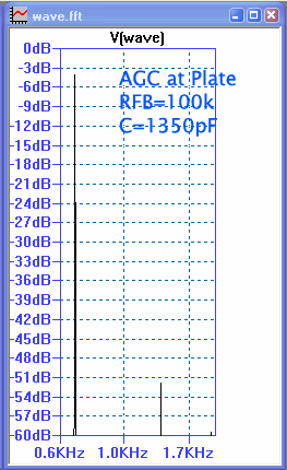
 The measurement on the left was done with for the first version at the top of this thread where the AGC circuit was fed with a more amplified signal from the plate. This resulted in overall lower oscillation amplitudes, which resulted in the 2nd harmonic being down -48dB from the fundamental. This is less than 0.5% distortion.
The second measurement was done with the constructed version at the low end of the x1kHz range. The AGC circuit takes it's signal from the screen grid G2 which results in higher amplitude oscillations. The 2nd Harmonic distortion is slightly higher at -45dB which is sightly more than 0.5%.
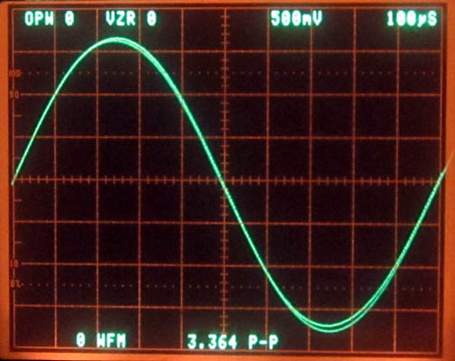
This scope photo shows a very clean looking 1kHz sine wave. You can see two versions of the sine wave superimposed. One is the inverted version of the other, but with the same positive slope trigger. If the sine waves had zero distortion, they would overlap perfectly and only one trace would be visible.
The slight deviation on the lower right explains the slight second harmonic distortion.
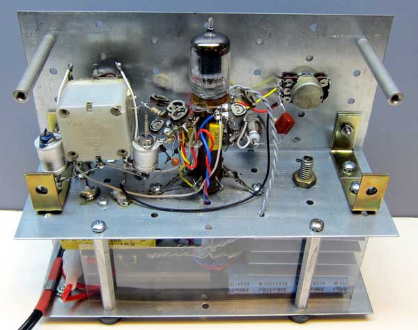
The constructed Single Pentode Wien Bridge Oscillator
The oscillator and it's power supply are housed in separate compartments. The power supply sits in the lower half with all components visible, but insulated with a plastic panel to prevent shocks from Bminus which is present at the low voltage selenium rectifier. The oscillator had to be completely shielded in the upper half to prevent hum pickup.
The construction material is soft steel plates that were made as nailing plates for wood beam construction. I have always found the hole grid very handy and it is easy to solder to the plates.
The main variable capacitor visible in the inside photos on the left sits at Bminus potential and is carefully insulated, including an insulation nut on the main shaft. The two insulated brass mounting holes in the front of the variable cap screw on to stiff paper clip wire, which is then bent to form a set of mounting posts that are soldered to the bottom steel plate. The barrel 30pF trim capacitors that are soldered on either side of the main variable capacitor were salvaged from a discarded Grundig radio. This is my favorite style of trim capacitor.
The 6SA6 dual control Pentode plugs into a prototyping turret with several posts along the barrel for interconnections.
The top shield was cut to size in a shear cutter and the hole for the tube was first punched out, then drilled out a little further. The side copper PCB panels were soldered to the top shield plate. This shielding assembly is held in place tightly by the front and back panels.
 |
 |
 |
 |
|
 |
Going Further
There are several aspects of the operation of this oscillator that could be improved. One is distortion, which is already quite good for a single tube RC oscillator, but I saw a fair amount of distortion variation from tube to tube, with the worst tube distorting 5%. The DC bias for the suppressor grid G3 might be adjusted for center the oscillations around the most linear part of the G3 operating range. Doubling the power supply range may also help with distortion, as oscillations could occupy a smaller proportion of the plate and screen G2 voltages. Forcing operation at an even lower oscillation amplitude by adding one more diode to serve as AGC voltage doubler may also linearize operation.
One particular aspect of the distortion I have not understood yet is that it appears to be a dominated by slope distortion, with the positive going and negative going slopes having different slopes. This is true for distortion levels between 1% and 5%. The surprising part of this distortion is that no delays are expected through the tube, but perhaps this is where I am misunderstanding the distortion mechanism.
The oscillation amplitude is a direct function of mains voltage. The amplitude sensitivity to mains voltage comes from the sensitivity of the control grid G1 transconductance (gm1) to heater and screen voltages. The addition of a 130V-150V shunt regulator for the high voltage supply would reduce the amplitude sensitivity to line voltage. The heater voltage could also be regulated the old fashioned way in a bridge circuit with a light bulb or ballast tube running a very different temperature than the heater. But perhaps the oscillation amplitude variations are not primarily caused by heater voltage variations.
The bulb controlled Wien Bridge Oscillator should have very little amplitude sensitivity to mains voltage because the controlling bulb characteristic depends exclusively on signal amplitude. The DC current flow through the bulb in some tube designs should degrade the amplitude immunity from mains voltage variations.
It is possible to build a functional version of this oscillator with an IF pentode with built-in detector diode like the EBF89, but the relatively small dual control range below the plate knee should cause higher distortion and the remote cutoff of the control grid should reduce the effectiveness of the AGC control circuit.
Acknowledgements
I designed this circuit about a year ago with a vague goal to publish it, but it was not until a private email exchange with RM member Robert Weaver about his amazing C-Quam AM stereo transmitter using valves, that he suggested I should finish and post this circuit. This resulted in the final construction and measurements.
It is impossible for me to think of Wien bridge oscillators without remembering the recently deceased Analog Guru par excellence Jim Williams. Jim was a student and great enthusiast of Hewlett's and Bernard Oliver's Wien Bridge oscillators and designed a recent version that achieved 3ppm of distortion. This oscillator was published in Jim William's last Application Note AN132 for Linear Technology. I can only imagine what a good laugh Jim would have had reading this post.
Best Regards,
-Joe
To thank the Author because you find the post helpful or well done.
Suppressor grid g3 bias adjustment
Fellow Radiophiles:
There was one loose end in the design of this oscillator that had to be settled. Different tube brands produce very different levels of distortion ranging from 0.5% to 10% in the worst case. When the distortion is increased, the frequency stability suffers greatly too, so this problem had to be solved.
I traced the source of the distortion to the variation in the center of the linear range of the G3-G2 transfer function. Adding a bias adjustment to the suppressor grid G3 made it possible to adjust the distortion below 0.5% for any of the 8 tube brands I tried.
The following schematic shows the new 5k potentiometer at the cathode circuit that serves to bias the suppressor grid G3 to obtain minimum output distortion. When adding the 5k pot to the 3 range circuit, all three frequency setting resistors RF1a, RF2a and RF3a must be wired to the 5k pot wiper instead of Bminus.
The 8 brands of 6AS6 I tried in this new circuit resulted in this range of optimum least distortion suppressor grid g3 bias voltages with respect to the cathode:
| 6AS6 Brand | Vg3k | R7=1.5K drop |
| (V DC) | (V DC) | |
| Russian | -2.9 | 2.00 |
| #32 Tung-Sol | -2.9 | 2.68 |
| #25 Dumont | -6.0 | 2.33 |
| #26 RCA | -3.5 | 2.38 |
| #34 GE | -4.1 | 2.57 |
| #30 Raytheon | -3.8 | 2.75 |
| Sylvania | -2.5 | 2.40 |
| #33 Amperex | -4.8 | 2.51 |
The -2.9V to -6V range of required voltages for suppressor grid g3 for minimum output sine wave distortion at the Vg3k column show the necessity for the g3 bias adjustment.
This variation is similar to the range seen in suppressor grid G3 bias in the Tomato Soup HI-FI AM transmitter.
However, the cathode current varies much less from tube to tube, as can be seen in the voltage drop across cathode resistor R7.
While exploring alternatives to generate the negative DC bias voltage for the suppressor grid G3 I was very surprised to find out that heater voltage has very little effect on cathode current, if the oscillator bias at G3 is adjusted for lowest sine wave distortion.
The following table shows the only 190mV variation at the cathode when the heater is varied 2V from 5.3V to 7.3V. This corresponds to a 10:1 cathode current rejection of variations to heater voltage. This is all the more surprising, considering that emission variations can be larger than heater voltage variations. While the emission variation in the Triode Emission column (Plate=G2=100V, G1=G3=0V) varies slightly less than the heater voltage variation from 5.3V to 7.3V, the emission variation from 3V to 7.3V is nearly 4 to 1, while cathode current varies only 8.6%. The Bplus voltage in the oscillator was kept at a constant 150VDC.
| Effect of heater voltage on Ik and Plate Sine | Triode | |||||||
| Vg3k=-2.9V for 0.5% distortion | Vg3k=-2V for 10% distortion | Emission | ||||||
| Heater | Cathode | Plate | Fo | Cathode | Plate | Fo | P=100V | |
| (VDC) | (VDC) | (Vp-p) | (Hz) | (VDC) | (Vp-p) | (Hz) | (mA) | |
| 7,5 | 7,72 | 41,23 | ||||||
| 7,3 | 7,70 | 40,81 | 474,4 | +1V | 8,44 | 39,64 | 490 | 17 |
| 7 | 7,67 | 40,27 | ||||||
| 6,5 | 7,62 | 39,26 | ||||||
| 6,3 | 7,60 | 38,77 | 474,6 | Nom | 8,19 | 38,26 | 484 | 15.5 |
| 6 | 7,57 | 38,16 | ||||||
| 5,5 | 7,52 | 36,89 | ||||||
| 5,3 | 7,51 | 36,88 | 474,8 | -1V | 7,98 | 37,01 | 479 | 14 |
| 5 | 7,47 | 35,62 | ||||||
| 4,5 | 7,41 | 34,10 | 12.8 | |||||
| 4 | 7,39 | 33,02 | 11.2 | |||||
| 3,5 | 7,32 | 30,77 | 9.4 | |||||
| 3 | 7,11 | 26,54 | 4.5 | |||||
| 2,5 | 6,42 | 14,38 | ||||||
| 2 | off | |||||||
The independence of the cathode current from heater voltage and cathode emission variations illustrates a fundamental point of the linear oscillation regime under AGC control. It is the purpose of the AGC control to keep the non-inverting voltage gain from G3 to G2 at 3x to satisfy the 1/3 loss through the Wien circuit. This means that the gm of the tube will be kept constant by the AGC loop, despite any emission variations. It appears then, that tube gm and cathode current are directly related, so that when the tube gm is forced for the gain-of-3, the cathode current is also forced to a fixed value, which in this case is nominally 7.60V/6.5k=1.17mA, regardless of tube emission.
But keep in mind that tube gm and current are kept constant at the expense of oscillation amplitude, which drives the AGC signal at the control grid G1. The oscillation amplitude varied greatly with heater voltage.
When I varied the Bplus voltage away from the 150V test conditions of the last table, the cathode current and oscillation amplitude both varied. This can be attributed to the G3-G2 gain also being a function of Bplus voltage.
The cathode current in this oscillator circuit could serve as a DC current reference source. The more linear the oscillation, the better the regulation of this DC current source. If a very linear triode oscillator were built with AGC control, then the sensitivity to G3-G2 gain would be eliminated and the triode current would be substantially independent of Bplus variation as well as emission variation.
Best regards,
-Joe
To thank the Author because you find the post helpful or well done.