6AS6 (6AS6) Suppressor action
6AS6 (6AS6) Suppressor action

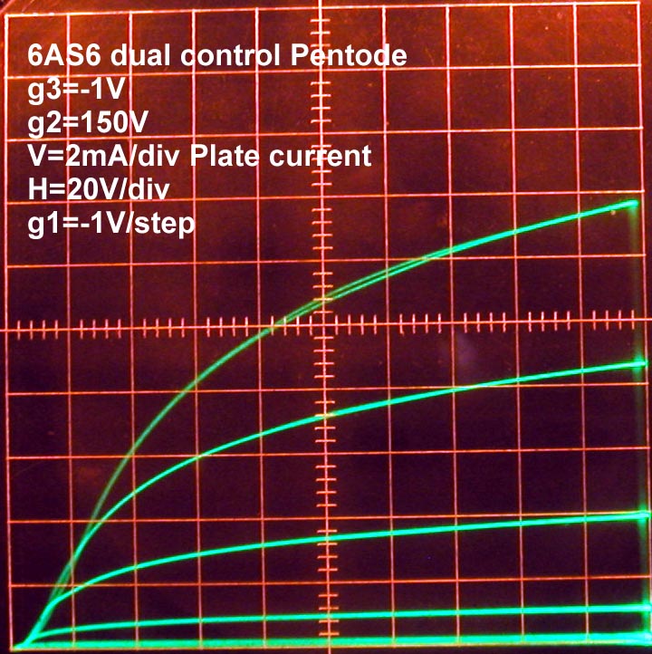
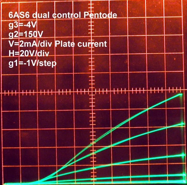
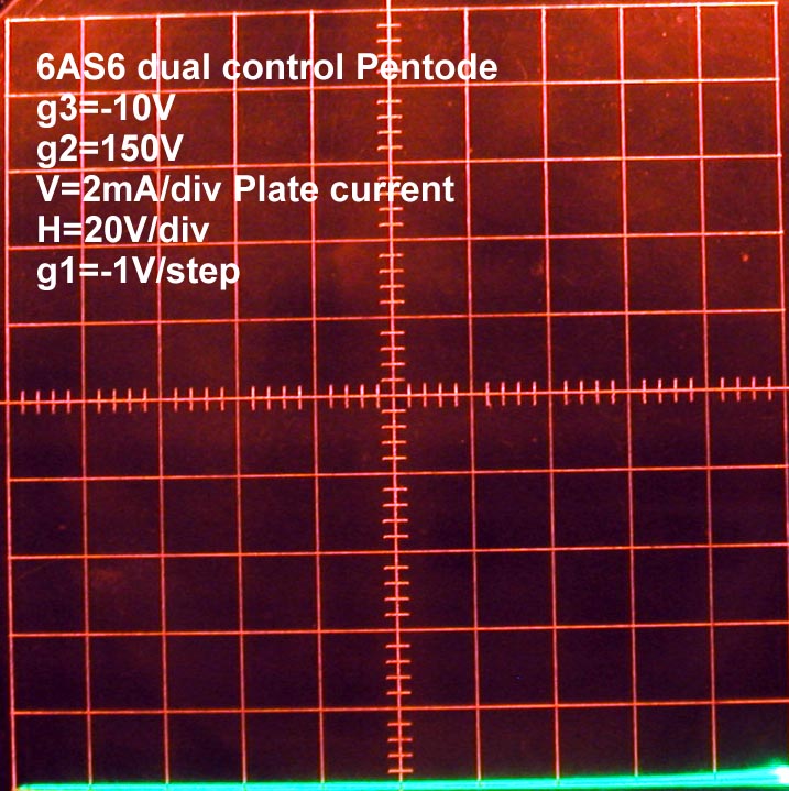
The following plots show the effect of bias voltage at the suppressor grid g3.


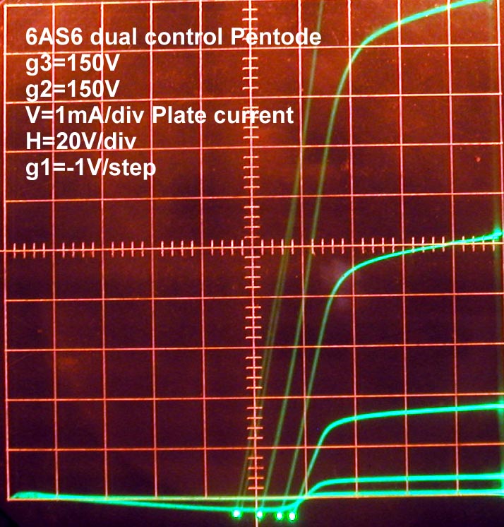
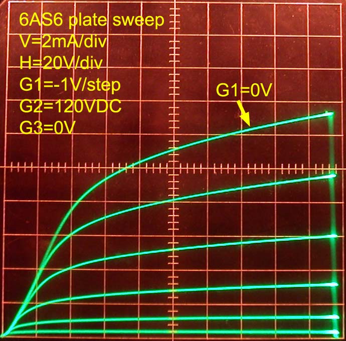
The 6AS6 was designed as a dual control sharp cutoff pentode. g1 and g3 both control plate current.
The following sequence shows the effect of g3 bias in -1V steps, on the classic plate current curve family with g1 steps.


Further discussion of g3 action can be found at:
http://www.radiomuseum.org/forum/app4120_gitter_1_3_parallel.html
http://www.radiomuseum.org/forum/6f6eg_6f6eg.html
Right-click and view or save these plots for higher resolution.
Regards,
-Joe
To thank the Author because you find the post helpful or well done.
6AS6 vs 6AK5
Fellow Radiophiles,
The construction of the 6AS6 and 6AK5 RF pentodes made by RCA is very similar, except for the suppressor grid G3. The following images were obtained with an Epson Perfection 1200u scanner at 1200dpi.


When I viewed the G3 suppressor grids under the microscope, they appear to have the same quasi-elliptical shape, made of two arcs anchored at the support rods. The only difference was the grid pitch. I count 7 grid wires for the 6SA6 in the same window that I count only 2 grid wires for the 6AK5. The reduction in the gap between wires is clearly greater than this pitch ratio.
Dual Control
The 6AS6 is designed for dual-control. This means that both the control grid G1 and the suppressor grid G3 have control over the plate current. As can be seen by the absence of a tetrode kink in the following plots, the suppressor grid of the 6AS6 still returns secondary emission back to the plate.
The combined effect of dual G1 and G3 control is a multiplication. This principle is behind multiplicative multi-grid mixers.
Suppressor Shielding
The tight screen pitch of the high mu 6AK5 pentode helps shield the action of the plate voltage on the current that flows to it. The loose grid of the 6AS6 allows the plate field to penetrate further into the space charge to control it. A higher plate voltage in the 6AS6 increases plate current much more than that in the 6AK5. When a resistive plate load is present at the 6AS6, any increase in plate current drop the plate voltage, which then drops the current somewhat, such that overall voltage gain is reduced, as compared to the 6AK5. The effect of the plate voltage on tube voltage gain is that of negative feedback, at least at low frequencies.
Curve family comparisons
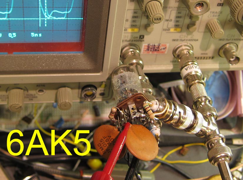
The next two photos show plate current for the 6AK5 and 6AS6 when the control grid voltage is stepped in -1V steps. These curves were traced on a TEK575 Transistor curve tracer.


This photo shows the controlling action that the suppressor grid has on the plate current. Note the nearly triode-like character of the curves. The flatening of the curves recalls the thermally limited emission of a triode when the entire space charge at the cathode has been eliminated by heavy current flow. In this case, it is the charge between the suppressor and screen that get depleted.

This photo shows the usual triode-like character of the screen current under the control of G1, with the plate at a high nominal fixed voltage.
Note that when the screen is at 120V, the transconductance to the screen is 2mS, which is very substantial when compared to the transconductance of 3.6mS to the plate at the same voltage.
The screen current saps over 1/3 of the transconductance that the 6SA6 would have, if it were triode connected, with plate and screen shorted.
The following two photos show that the suppressor grid G3 has a -0.5mS transconductance effect on the screen grid G2. The first plot sweeps G3 in -1V steps and the second plot shows the effect for +1V steps. Note that there is substantial G3 conduction during the positive steps. The negative transconductance from G3 to G2 results in a non-inverting voltage gain.

Unfortunately, the suppressor grid G3 of the 6AK5 is internally hard wired to the cathode, so I can't make a direct comparison of it's effect on the screen current. However, I will show the effect on another conventional single G1 control pentode, the EBF89.
The next plot shows the controlling action of G1 in -1V steps, and the following plot shows the relatively small controlling action of G3 in -1V steps.

If the curve tracing is zoomed in on the left side of this last plot, where most of the G3 control action occurs at low plate voltage, we see a striking similarity to the G3 curve family for the dual control 6AS6 above.
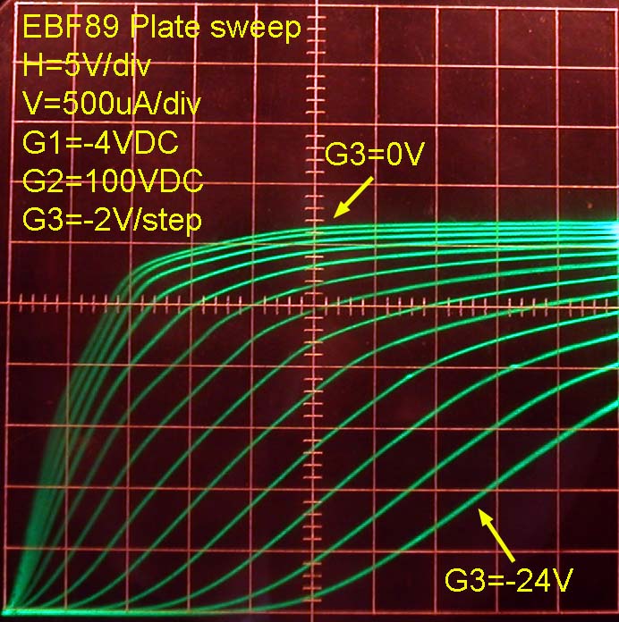
This plot shows the first 50V of the 200V plate sweep of the previous plot.
Note that significant transconductance from G3 to the plate does not occur until G3 is more negative than -5V.
At the top of the curve family, there is a relatively small space charge behind the tightly spaced G3 grid that the plate can fully deplete. The suppressor voltage is above -5V. All controllable charge behind the suppressor is depleted when the plate curves are horizontal.
As was seen in this series of suppressor grid action measurements, various pentodes that were designed for G3 to be grounded, respond differently to G3 voltage variations. Some pentodes that were not designed for dual control will respond to G3 if the plate voltage is kept well below the screen voltage.
The principal reason why G3 was often brought out on an external pin was for AC performance. When G3 and the Cathode share a pin, the plate to cathode capacitance is increased, and this makes any parasitic inductance in the cathode connection affect the HF response of the tube. The topic of separate connections for G3 and K has been addressed several times in this forum, and most recently by Prof Rudolph. (I used Google-Translate to read this German language post)
Step responses
The following TEK2467B scope photos show the G1 and G3 step responses for the 6AK5 and 6AS6 as seen at the plate.

The PG502 pulse generator drives a 50MHz square wave between 0V and -2V. The input and output are simultaneously shown on the scope but with the grid drive input inverted for easier comparison of delays and rise times. The 0V line for the grid is marked with a flat trace.


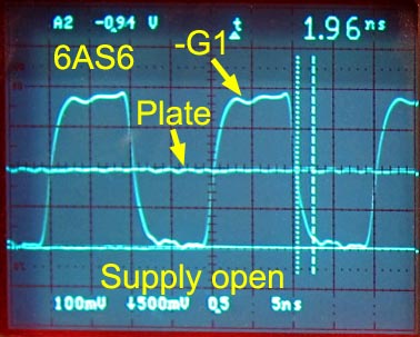


The step response from the control grid G1 to the plate is very similar for both 6AK5 and 6AS6.
I was surprised to find out that the delay for the suppressor grid G3 step response is as sharp and with the same delay as the response from G1. This implies that the space charge that G3 controls is very close to it, perhaps at the same distance that G1 is from the space charge around the cathode.
The reduced amplitude of the G3 response reveals it's lower transconductance.
To the right of the G1 and G3 step responses I show the responses when the 120VDC source is disconnected. This shows any feedthrough effects from parasitic capacitance. The G3-Plate capacitance feedthrough causes observable feedthrough in the last scope photo.
Curves for other pentodes available at suppressor grid action measurements.
Regards,
-Joe
To thank the Author because you find the post helpful or well done.
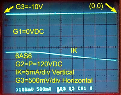
Control Grid and Suppressor Grid Sweeps
Fellow Radiophiles,
I took an additional set of curves for the transfer functions from the two input grids G1 and G3, to the Screen grid, Plate and Kathode. These curves were done without the Tek575 curve tracer that was used for the plots above. The Plate and screen voltages were kept at a constant 120V, while input voltages were swept one at a time, and output currents were displayed.
The first plot shows the familiar kathode current under control grid G1 sweep. The second plot shows the kathode current again, but under suppressor grid G3 sweep. Note the small transconductance (slope) that G3 has on total cathode current.

The next two plots repeat the G1 and G3 sweeps, but show the Plate and Screen grid G2 currents.
The first plot shows nearly equal plate and screen currents under G1 sweep when G3 is grounded.
The last plot shows a transconductance of +1.4mA/V=+1.4mS for IP, but -0.9mA/V=-0.9mS transconductance for IG2.
IK= IP+IG2
The positive transcondcutnace from G3 to Plate results in the familiar inverting voltage gain under resistive loading.
The negative transconductance from G3 to G2 results in non-inverting voltage gain under resistive loading.


The behaviour outlined in this thread is very typical of all dual control pentodes.
Regards,
-Joe
To thank the Author because you find the post helpful or well done.
Non-inverting Step response from G3 to G2
Fellow Radiophiles,
I was very curious about the non-inverting step response from the Suppressor grid G3 to the Screen grid G2 while the Control grid G1 is grounded and the Plate is at a fixed 120V potential.
The following scope photos reveal that the delay from G3 to G2 is comparable to the ~2ns delays shown above from G3 to the Plate and from G1 to the Plate.


 The first photo shows the step response from G3 to G2 with 120VDC applied to the Plate and to G2. A large overshoot spike is prominent. This spike is caused by the capacitance from G2 to G3.
The spike effect of this CG2G3 is very clear when the 120VDC power source is removed.
The last shot superimposes the two previous shots to show that during the spike there is no transconductance response from the tube because the spikes are nearly identical.
It can be concluded that the delay from G3 to G2 is about the same 2ns that was seen for other delays in this tube.
The ~2ns delays observed within the 6AS6 and 6AK5 tubes are the dominant factors limiting the high frequency gain of these tubes. But these delays also complicate any needed neutralization, because a purely inverted signal for neutralization, without some phase delay, is no longer possible, unless reactive elements beyond what is needed for neutralization are used. This problem was addressed in the legendary study of the Grundig 5040W/3D by Herr Hans Knoll in post 36 of part1 in the English translation by Mr. Thomas Albrecht of the original German post 28 part1, which was moderated by Herr Thomas Günzel.
My curiosity to measure this delay was driven by the fact that G3 exerts a retarding field over G2 that affects the current flowing into G2. The retarding field might return some electrons that have passed the Screen grid G2 back to G2, or it could be that attraction to the plate is reduced by G3, so that more electrons go directly to the Screen grid G2. A determining factor for which set of forces is dominant is the momentum of the electrons near the screen grid G2. My understanding of space charge behviour is enough to ask the question, but not enough to answer it.
Any further information on retarding field action of this nature would be welcomed.
Regards,
-Joe
To thank the Author because you find the post helpful or well done.