Boost Converter HV Supply for Battery Radios
Boost Converter HV Supply for Battery Radios
There have been a number of discussions on this forum about replacements for B batteries for the anode supply of radio receivers. For my own battery radios, I had initially adopted the common practice of snapping together several 9 volt batteries in series and using those. Since many battery radios have modest power requirements, these will last for quite a while before requiring replacement. Eventually though, I thought it might be more convenient to use a lower voltage higher capacity rechargeable battery driving a boost converter. I experimented with a few different boost converter circuits. Integrated circuits designed specifically for boost converter service, I found to be very tricky to implement. After much failure, I decided to try more generic parts. My first success was with a TTL 74123 dual monostable multivibrator, with one of the multivibrators connected as a free running oscillator, which then drives the second as a pulse width modulator.
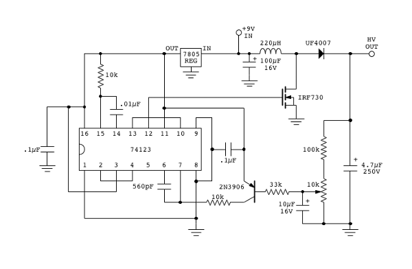
I decided to go with the dual multivibrator circuit so that I could predetermine the switching frequency. It is determined by the timing resistor and capacitor of the first multivibrator, and doesn't vary, regardless of the load. I thought this might be a useful feature so that I could pick an operating frequency that would minimize interfering harmonics. The circuit worked reasonably well, but the efficiency was not very good. The TTL IC required a regulator to keep the supply voltage at 5 volts, and the TTL IC itself drew quite a bit of current. These things contributed significant overhead to the power consumption. Eventually, I replaced the 74123 with an ICM7556, the CMOS version of a dual 555 timer.
 Because it's CMOS, this IC draws much less power than the TTL IC, and it doesn't require a regulated supply, because it has a wide supply voltage range. Other than that, the circuits are nearly identical in operation. One half of the ICM7556 is a free running astable multivibrator, which triggers the second half connected as a monostable multivibrator. Voltage feedback is via the bipolar transistor which controls pulse width. The remainder of the circuit is fairly standard boost converter topology, and so I won't go into details for that part.
Although it is CMOS, the 7556 has quite a high drive capability, so that it has no problem driving the highly capacitive gate load on the MOSFET. The CMOS version of the circuit has an efficiency of more than 80% when it's up-converting from 9 to 90 volts and delivering 25 mA to the receiver. This is approximately the supply requirements of a Zenith TransOceanic R600 receiver.
This circuit, by the way, can be adjusted to deliver up to 450 volts, though I have not done any significant amount of testing to find out maximum current and efficiency at this voltage. The following photo shows the two boost converter circuits: the 74123 TTL version on the left, and the ICM7556 version on the right.

After getting the boost converter to work reliably well, the next issue to address was the RFI introduced into the receiver due to its switching harmonics. Reports from a number of people seemed to be rather discouraging, but I reasoned that with enough shielding and filtering it should be possible to clean up the supply acceptably well. I found that by completely shielding the entire converter and using the following output filter, the RFI was reduced to acceptable levels.

In this filter, the inductor is wound on a high mu (µ=6500) ferrite toroid.
Though the RFI is not quite inaudible—it comes in faintly at periodic locations across the band—it doesn't seem to cause any serious problems even on weak distant radio stations. There is still room for improvement though, and I plan to do more work with the filtering. I believe that one or two additional filter stages similar to the one shown above, should reduce RFI to insignificant levels.
There is one remaining issue, and this is what I have been working on recently. The boost converter needs to be switched on and off separately from the rest of the radio. And this can be an inconvenience. It is certainly possible to add some internal wiring to the radio using the filament voltage after the switch, inside the radio, to operate a relay and turn on the boost converter. However, it would be much better to have something that doesn't require invasive modifications to the receiver. The only other option then is to monitor the current of the filament supply battery, and when current flow is detected to the filament circuit, then the B battery boost converter is switched on. The simplest solution would be to use a sensitive current relay. This could be practical with a reasonably high current filament load, but again with the example of the Zenith TransOceanic R600 receiver, the filaments of the tubes are wired in series, and the total current is only 60 mA. I wasn't able to find any relay sensitive enough to switch at less than 60 mA without causing a significant voltage drop in the filament circuit. So, I decided to develop a more sensitive solid state current sensing circuit.
The design of the filament current sensing circuit poses one significant challenge. When the radio is off, then this circuit must not consume any power. The circuit to be described here draws only about 40nA (nanoamps) when the radio is off. This is probably less than the current that would leak from the battery due to imperfect insulation in the battery itself. Consequently, the battery should last for its normal rated shelf life when the radio is off.
To achieve this very low power consumption, the circuit has two separate modes of operation. The first mode is the ultra low power mode in which it operates when the radio is off. Referring to the schematic below, the voltage on the line labeled "Switched Ground Bus" is controlled by the output of NAND gate U1b. When the radio is not drawing any filament current, the output of this NAND gate is equal to the positive battery voltage. This puts every point in the circuit, except one, at the positive supply voltage. Since everything is at the same voltage, there is no potential difference, and therefore no current flow. The only exception is the quiescent current of U1 which is 40nA. Note that pin 7 of U1 is the only part of the circuit that is connected, via ground, back to the battery negative terminal.

With the radio drawing no filament current, both inputs to U1a are at logic 1. Its output is logic 0, and U1b connected as an inverter, then has an output of logic 1 as previously stated.
When the filament load is applied, it is a much lower resistance than R5, and so the voltage at point X (upper right of the schematic) drops to near zero volts. The voltage at pin 8 of U1 starts to drop, delayed by the time constant of the R6-C1 network. When it reaches logic 0 voltage, the output of U1a changes state to logic 1, and consequently the output of following gate U1b goes to logic 0, or ground potential. This pulls the switched ground bus down to true ground potential, thus activating the rest of the circuit. Since one side of C1 is connected to the switched ground, this provides a positive feedback effect, pulling pin 8 of U1a down hard, and preventing the possibility of it drifting back up to an indeterminate logic state before the rest of the circuit becomes operational.
With the switched bus at ground level, the current sense amplifer U2 (Silicon Labs Si8540) is now operational and begins sensing battery current flow. The gate of the P-channel MOSFET Q2 is now grounded, switching the transistor on fully, bypassing the 10k current limiting resistor R5 and thus applying full voltage to the radio’s filament load. The filament current is now sufficient to cause the output of current sensor U2 to rise, switching on transistor Q1 which pulls down pin 9 of U1a to logic 0. At the same time, pin 8 of U1a is starting to rise, but as long as one of the U1a inputs is at logic 0, the output of U1a will remain high, and the switched bus will remain at ground potential. The circuit has now fully changed over from its ultra low power sensing mode, to a higher current operating mode, with U2 now providing the load current sensing.
The output of U1a also goes to the inputs of gates U1c and U1d whose outputs are connected in parallel and act as a buffer stage. Their outputs are now at logic 0 state, and energize the coil of relay K1, which switches on the B supply boost converter. All power is now available to the radio receiver.
When the radio is switched off, the filament current drops to zero, and this is sensed by U2. Its output drops, switching off transistor Q1, which causes pin 9 of U1a to go to logic level 1. Pin 8 is already at logic 1, and so U1a output goes low. This causes the output of U1b to go high, bringing the switched ground bus back up to the positive supply voltage. Relay K1 drops out, shutting off the B supply boost converter. The circuit is now back in its ultra low power state.
The circuit, as presented, is sensitive enough to sense current flow of less than 30 mA. This is plenty of safety margin, since the lowest filament current in common production vacuum tubes is 60 mA. The tubes in the Zenith Transoceanic, for example, are all 60 mA filaments. The six tubes in this receiver have 1.5 volt 60 mA filaments which are connected in series for a net 9 volt 60 mA load.
Zener diode D2 may or may not be required in the circuit, depending on the the voltage of the filament supply battery. For a 6 volt battery, D2 may be replaced with a jumper. For a 9 volt battery as would be used with the Zenith TransOceanic, the 3.6 volt zener should be used, because the relay coil is rated at 5 volts. The amount of current that can be delivered to the relay coil is also limited by the maximum current capability of the CMOS gate output. So, it’s unlikely for any damage to occur to the relay, in any case. But this puts less stress on the CMOS gate output. For higher filament battery voltages, the zener diode voltage rating should be about five or six volts less than the battery voltage.
The following photo shows the completed current switch circuit board.

Edited to add the following additional information on the components used in the above circuits.
In the boost converter circuits:
High voltage diode is part No. UF4007, an ultrafast rectifier. It is available from several manufacturers such as Vishay and Fairchild. Though the part number is very similar to a 1N4007, the parts are not equivalent, and a 1N4007 cannot be used.
The inductors are Coiltronics DR127-221-R, or AlfaMag SWF-1.4-220. Both types were tested in the circuit and gave similar efficiency.
The CMOS dual timer ICM7556 is available from several manufacturers, though the 'ICM' prefix used by Intersil varies with other manufacturers.
In the Current sense switch:
U1 is a CD4011 quad 2-input NAND gate, standard low speed CMOS logic. The high speed versions such as 74HC4011 should not be used because they will not have the required low quiescent state current draw. Nor will they have the wide supply voltage tolerance of the low speed version.
U2, as mentioned above is a Silicon Labs Si8540 current sense amplifier. This puts out an analog voltage proportional to the sensed current. Because of the analog signal, it is followed by Q1 which converts it to a 0/1 logic signal.
Relay K1 is a Hamlin HE721A0500 reed relay in a DIP form factor. I am currently looking at the option of using solid state relays such as the Vishay LH1518 which appears to have a suitably low off-state leakage. On the PC board, a socket has been provided for the relay so that an alternative device may be easily substituted.
Edited 2016-04-25 to add printed circuit layouts for the ICM7556 boost converter, and the current sensing switch.
See attachments below. Note that the foil patterns are mirror image so that they are suitable for toner transfer type fabrication.
(For the current sensing switch, component U2 is a surface mount device and is mounted on the foil side of the circuit board.)
Attachments:- Boost Converter Foil Layout (20 KB)
- Boost Converter Component Layout (39 KB)
- Current Sw Foil Layout (33 KB)
- Current Sw Component Layout (45 KB)
To thank the Author because you find the post helpful or well done.