Transistor Connections
Transistor Connections
 Günther Stabe writes
Repeated problems arise when considering the naming or identification of the semiconductor connections and their assignment to the line drawing ("base image") on.
Alone in the TTT of 1981 (Steidle) about 600 designs, each with 18 different port .. first names are mentioned, it is already a lot of old forms no longer listed. There are also countless new forms of the past 30 years, so it also for the specialist to be a little too over-looking variety.
[Currently JEDEC lists about 3000 packages!]
As each country and usually each manufacturer's own "forms" (outline) developed and thus determined the counting order, it was important for the correct assignment to be able to acquire such knowledge or look up. This inevitably leads to a jumble of "Left to Right", "right to left", "inside out", "clockwise", "counter clockwise" etc.
Therefore, I remembered a tip in the past from a former classmate:
- Color point (if it exists, right)
- middle connector (usually base) to the top
- from left to right
Conclusion: it's probably not really ...
The first image below is the common "base" forms of the types of connection [including some of the oldest]. These are types of wire or pin connector, regardless of the housing material. This changed often during the production period.
Please note the types of heat sink assembly, e.g. TO-3, TO-66, SOT-9, etc., there were 2, 3, 4 or more connector pins, so it is relevant to the drawing - if available or known -
So, if you read the descriptions of the types of semiconductor RMorg the text "... connection sequence BEC" (always: view from below, unless otherwise noted), is unavoidable . It is always "subject to error," because I often have at least four sources match to reach the "correct" outcome. Also, different manufacturers of the same type have used other sequences (!). Therefore, I ask in difficult cases in a message to be patient, it may be that I need a longer time for data collection and clarification ...
- TO ... Transistor Outline
- DO ... Diode Outline
- SO .. Small Outline (transistor / diode / Plastic)
Historically Valve (Tube) bases were shown from below (though on CAD systems are often shown in reverse, from above) and apart from maybe C35 base numbered clockwise. This is often but not always true for transistor packages (the start at left if "curve at top" and at right if "curve at bottom") ICs are always numbered like tube bases, but from top view, so the numbers run anti-clockwise, but "base" view is the same as valves/tubes.
T0-92 and similar small plastic packages are the worst with all possibilities existing of CBE, EBC, BCE, ECB, BEC and CEB,
Transistor pin identification
Using a 350V source limited by 2M ohm resistor such as a leakage tester you can identify the BE vs BC junction as the Base Emitter is about 5V to 15V breakdown (Zener) and the Collector Base about 20V to 150V (or even 1000V) breakdown (Avalanche). Providing that neither current or power is exceeded this should not damage the part. A DMM (Diode or Ohms) or AVO (ohms) can identify which pin is base and if it's PNP or NPN. many DVM will display junction voltage.
Diodes
Dual diodes can be in a transistor package. These can be in series (switches or modulators) or can be common cathode or common anode.

Uploaded by Günther Stabe
Types of Semiconductor in Transistor & Diode package
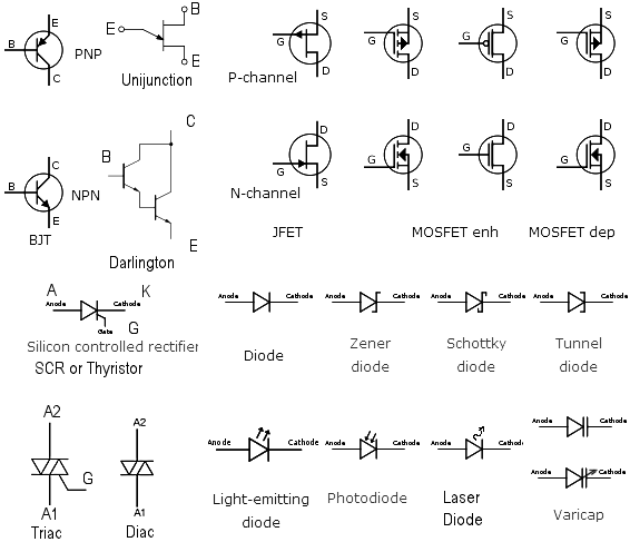
As noted above varicaps, regular diodes, PIN diodes, switching diodes etc are often in a transistor package.


Ge Power Transistor packages. Click for full size.

Common connections.
Data sheets often show the "curve" at the top.
The SOT23 is common for two diodes, middle pin can be K+K, A+A or K+A

Common cases See Heatsink note
(click for full size)
Note that power devices with plastic/ceramic parts (TO126, TOP-3 aka TO3-P, TO220, TO247), are normally drawn with the part that mates with heatsink facing away, but all metal parts such as TO3 and TO66 are drawn with pins and heatsink facing the viewer. The larger space pins (TOP-3, TO247 and others) usually have the centre pin connected to tab. When the Tab of the larger plastic/ceramic parts mounted on one of the holes of the TO-3 heatsink the middle pin can be cut short and the B and E pins will be correct spacing and orientation to bend through the TO-3 B and E holes in the heatsink.
RF transistors are almost always drawn "top view" i.e. the heat sink mounting surface facing away like normal TO-220 view.
To thank the Author because you find the post helpful or well done.
Older Germanium packages
Some 1954 and earlier Germanium packages


To thank the Author because you find the post helpful or well done.
Some more outlines
From old Cirkit/Ambit catalogue in 1980s (Company long gone)


To thank the Author because you find the post helpful or well done.
Some Diodes

Note the "snap apart" packages are single 2 pin transistor style when fitted in a PCB. They are only 6 pin or 4 pin strip when new to ensure a matched set.
To thank the Author because you find the post helpful or well done.