Cathode Ray Tube Memory (RAM)
Cathode Ray Tube Memory (RAM)
Before the advent of the magnetic core store system for fast read and write computer memory (RAM), the most sucessful was the CRT system.
This relies on the fact that a small electrostatic charge appears on the inside face of the cathode ray tube where the electron beam hits the surface and that this charge remains for a short period of time before leaking away.
The presence or absence of this charge can be detected; when the beam again strikes the same area there is a difference in the small voltage appearing on the outside of the face of the tube.

A standard but selected radar display tube was used. On the drop-down cover can be seen the circular metal disc which was placed in contact with the front of the screen and which picked off the charge. The whole assembly had to be very well screened to prevent external interference.
By scanning the tube area it is possible to store multiple data bits and to rapidly read them. A system of continuous read and re-writing is required to preserve the data.
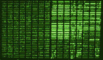
This shows a typical display on the tube face. Because the actual storage tube was fully enclosed a repeater tube and display was used.

This enabled a clearer display to be achieved.
The scheme was patented in 1946 by Dr F C Williams and developed in conjunction with Tom Kilburn and Geoff Tootill over the next two years before incorporation in the Manchester (UK) Mark 1 computer which was commercially developed as the first Ferranti machine.
The Williams-Kilburn tube was also used by IBM.
The Selectron tube was developed at about the same time and also used the principle of charge storage. However, the Selectron was a complicated and expensive item to manufacture and over the period 1946 to 1948 did not reach viable production which led to the use of the Williams-Kilburn tube despite having only 2k bits memory instead of the 4k of the Selectron.
To thank the Author because you find the post helpful or well done.
The CRT memory developed by US NBS

In December 1953, Electronics described the CRT computer memory array developed by US National Bureau of Standards. Even if Williams and Kilburn explained the operation of their system, basing upon the well-known theory of secondary-emitting surfaces, there were some not well-explained phenomena. Nevertheless, CRT memories, based upon the Williams storage system, were widely used for their high speed. In US, to take full advantage of their speed, memory banks were often built with a word-wide parallelism. In this case, a battery of 45 cathode ray tubes was used to store words wide 45 bit each. Read or write speeds of 21,000 words per second were obtained. By the way, similar speeds were also obtainable with some delay line memory units.
Several cathode ray tubes were satisfactory tried in the described array, 5UP1, 5UP11 and also 3KP1. Here are some pictures of the memory, showing a group of CRTs and details of a pair of tubes with shields removed; in these pictures also video amplifiers are visible below CRTs. The third picture shows the pattern of stored bits on a repeater monitor.

-----

-----
A dot-dash mode of operation was chosen, dashes being written for the ‘one’ locations. The X and Y deflection plates of the 45 CR tubes were connected in parallel, driven by a staticizer/counter with two power DACs. 4 bits were used for the X-axis and 5 bits for Y, resulting in a total capacity of 512 words. Each DAC used three 807s in the output stage, to drive an equivalent load of 1200pF through a 100V swing, with 3µs settling time. A sequencer generated a 0.5µs write/read pulse to drive the grids of the CRTs, plus a 0.25µs read strobe pulse and a ramp superimposed on the Y deflection signal. If a ‘one’ was detected on the read strobe, the write pulse was stretched to 2.5µs. A block diagram of the memory system is given below, together with simplified schematics of the gating amplifier, which has a gain as high as 30,000, and of the X deflection circuit.

-----

In this system stored data need to be continuously regenerated: this function involves sequentially all the memory positions and is intermixed with the computer access. Every location access takes 12µs, regardless of whether it is a read/write or a refresh cycle. Therefore a new refresh of the entire array takes place every 6144 microseconds.
To thank the Author because you find the post helpful or well done.