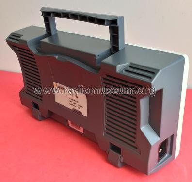
Two Channel 100MHz Digital Oscilloscope SDS1102
Owon; Xiamen Lilliput Technology Co., Ltd; Softpack, Xiamen
- Fabricante / Marca
- Owon; Xiamen Lilliput Technology Co., Ltd; Softpack, Xiamen
- Año
- 2017 ?
- Categoría
- Aparato de medida y servicio (Equipo de laboratorio).
- Radiomuseum.org ID
- 324573


Bought in Oct-2020


Haga clic en la miniatura esquemática para solicitarlo como documento gratuito.
- Gama de ondas
- - no hay
- Tensión de funcionamiento
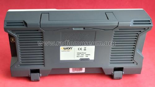
- Red: Corriente alterna (CA, Inglés = AC) / 100-240 50/60Hz Volt
- Altavoz
- - - No hay salida de sonido.
- Material
- Plástico moderno (Nunca bakelita o catalina)
- de Radiomuseum.org
- Modelo: Two Channel 100MHz Digital Oscilloscope SDS1102 - Owon; Xiamen Lilliput
- Forma
- Unidad para estanteria.
- Ancho, altura, profundidad
- 301 x 152 x 70 mm / 11.9 x 6 x 2.8 inch
- Anotaciones
-
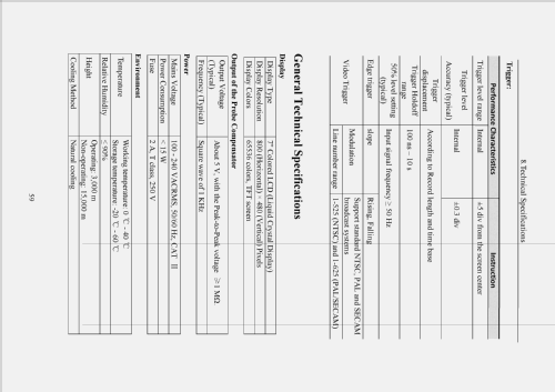
Owon two channel digital oscilloscope SDS1102. Main features:
- 7" LCD display, 800 x 480 pixels
- 100 MHz bandwidth
- 1 GSa/s sample rate
- 10 K pts wavelength
- Vertical: 5mV/div - 5V/div, 8 bits resolution
- Horizontal: 2ns/div - 1000s/div in 1-2-5 scale
- Trigger: Edge or Video, Auto, Normal, and Single
- Waveform Math: +, -, x, ÷, invert, FFT
- Storage: Internal and external USB storage (at front panel)
- Connectivity via USB to Windows 10 PC with OWON application for remote capture of data and remote control.
See also the same model Owon SDS1102 manufactured for the German brand Pollin.
- Peso neto
- 1.1 kg / 2 lb 6.8 oz (2.423 lb)
- Autor
- Modelo creado por Jose Mesquita. Ver en "Modificar Ficha" los participantes posteriores.
- Otros modelos
-
Donde encontrará 5 modelos, 2 con imágenes y 1 con esquemas.
Ir al listado general de Owon; Xiamen Lilliput Technology Co., Ltd; Softpack, Xiamen
Colecciones
El modelo Two Channel 100MHz Digital Oscilloscope es parte de las colecciones de los siguientes miembros.
Contribuciones en el Foro acerca de este modelo: Owon; Xiamen: Two Channel 100MHz Digital Oscilloscope SDS1102
Hilos: 3 | Mensajes: 5
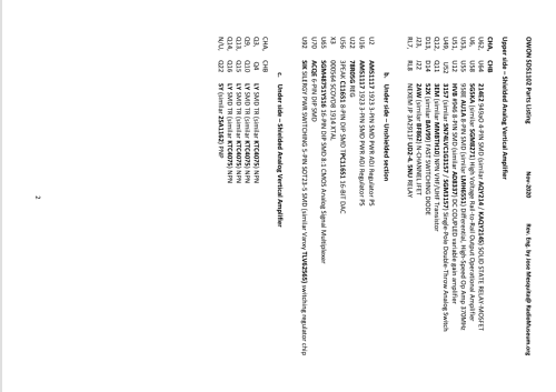
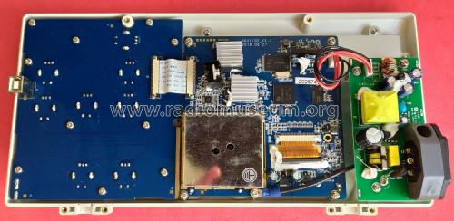
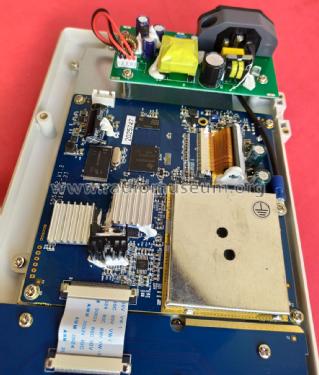
In order to list the active components use in this equipment, I have done a complete teardown.
The two aluminium heatsinks covering two LSI chips are hiding the FPGA and the ADC.
The FPGA at position U7, is a popular Xilinx Spartan-6 XC6SLX9.
The ADC at position U45, is a Analog Devices HAD1511, 8-bit, 1 gSpS, A/D Converter, single/dual/quad channel. It uses the U46 8V97051 Wideband RF Synthesizer/PLL VCO to sample the analog signals coming from both vertical channels U53/U55 AU1A (similar to LMH6551) Differential High-Speed 370MHz Op Amp.
Besides the LMH6551 opamp, each vertical analog amplifier uses a SG5KA (similar to SGM8271) High Voltage Rail-to-Rail Output Operational Amplifier, a HVB (similar to AD8337) DC COUPLED variable gain amplifier, a 3157 (similar to SGM3157) Single-Pole Double-Throw Analog Switch, a 3EM (similar to MMBTH10) NPN VHF/UHF transistor, a 52X (similar to BAV99) FAST SWITCHING DIODES for circuit overload protection, a 2AW (similar to BF862) N-Channel JFET, and a NEXEM UD2-4. 5NU RELAY.
Additional active components for auxiliary functions are seen in the main PCB, like a a C116S1 (similar to TPC116S1) 16-bit DAC, a SGM48751YS16 8:1 CMOS Analog Signal Multiplexer, two TP2274 ICs 36V CMOS OPAMPS with 4 opamps each at 7MHz bandwidth, and a bunch of NPN and PNP fast swirching transistors (mostly LY/KTC4075 and SY/2SA1162.
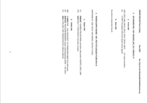
Quite a lot of local power supplies are used in the main PCB, on both sides, required to generate the different operating voltages of the active circuits. This approach optimizes the power decoupling and filtering, while allowing to use a single 15 Watt, 5.5 Volt, Switching Power Supply on a dedicated PCB.
This 5.5V SPS runs from 100-240VAC that is rectified by the BR1 JF ABS8 0192 (800V, 0.5A, 30A peak) full bridge, and uses a PN8149 8-pin PWM controller with power MOSFET IC that can handle a maximum of 24W, driving a step-down transformer (ref. 0201-0643). The loop uses a PH1 EL817 B017 4-PIN PHOTO-transistor coupler. A single D3 SEMIKRON K45 R15 power switching diode (SK45 --> 4A, 50V) and three capacitors shapes the 5.5V output to power the Main PCB and KEY Board PCB.
The Main PCB, upper side, having the IC's heatsinks and Analog Amplifiers shielding removed:

Analog amplifiers exposed after removing the shield:

Main POCB under side:

Jose Mesquita, 05.Nov.20
I left my scope running non stop since yesterday, more than 12 hours now, sampling a ~20MHz ~90mVrms RF signal in FFT mode.
Nice and stable for such a low level signal considering this is a low cost scope.

And now injecting a RF signal at ~110MHz and the scope acquires it reading ~78mVrms, not bad for a 100MHz scope!
I can not test it above 110MHz because my old vintage Heathkit 1G-102S is it its maximum frequency now.

Jose Mesquita, 16.Oct.20
Recently I bought one of these OWON SDS1102 2-channel scopes.
1. Small intro.
Having worked in electronics since the 70's on several different fields from radioisotopes labs to telecommunications, I had my fair share of professional equipment from brands like Tektronix, HP, RACAL, FLUKE, and so on, and it is easy to lose perspective of things when you are spoiled with 1GHz real time oscilloscopes in the 70's, some with storage memory.
2. Is this OWON SDS1102 a low cost scope, as advertised in their own website?
Yes, absolutely.
OWON is honest in what they are advertising.
3. Is it garbage?
Not at all.
For the asking price (I paid 190 EUR delivered from Spain on AliExpress) I can not ask better specifications and above all, real performance above what people may think.
It is an honest product, very useful when you need a dual trace scope with memory to do some basic repairs or adjustments on consumer electronics or even on professional equipment, why not.
The integrated counter and meters are spot on, I have checked it against my calibrated 520MHz vintage Fluke 1920A.
4. Is it badly designed and built?
Not at all.
If you are into electronics and have experience and knowledge on design and build equipment, you will recognize that this design is on pair with any other brand design on the same price range.
Do not get fouled by the apparent simplicity when you remove the back cover and look to the three main assemblies.
This is a modern design, well laid out, properly shielded where required. It has nothing to do with lesser integrated designs that use bigger components and huge metal cans that give you a feeling of robustness, surely, but that has nothing to do with real performance of that product.
This is a complex design, miniaturized with SMD components on BOTH sides of the PCBs, and made as simple as possible without compromising the specs and performance.
In fact, it is impressive built considering the price point.
5. Are there compromises in design and implementation?
Sure, there are.
But you will find them in any other oscilloscope, irrespective of price range. You will want more. That is the human nature.
On this design, the analog vertical amplifiers and ADC could have 1mV/div instead of that 5mV/div with limited bandwidth, and the trigger could be more efficient to handle RF audio modulated signals.
On this implementation, the switching power supply could have been enclosed in a metal can. But again, why people, like myself, tell this? Did we actually took measurements on using shielded power supplies in this model? That is assumptions we made, without any proof.
Talking about power supply on this model, some reviews mention on how simple the power supply is, like a more complex design would be better. Again, that is an assumption without any proof.
The implemented power supply achieves the required specs with safe margin, and it is not as simple as people may think. The PCB has components on BOTH sides.
Additionally this SDS1102 model uses LOCAL Regulated power supplies close to the respective loads (look closer to the main PCB).
Do I like to see a huge electrolytic cap mounted over the main PCB in piggyback style, like they had second thoughts about the implementation?
No, I do not. But looking into other OWON models and PCB revisions, I understand that that decision is deliberated, probably to save precious PCB space and maintain the manufacturing costs in check.
The plastic injection used for the case components looks good to me, but it could be better. On my unit, the handle is warped a little on one side. Small thing, but enough to show where they cut costs.
6. Wrap up
That is all, folks.
This is my honest findings so far.
Others will have other opinions about this scope after they have used it for a while, I respect that.
Jose Mesquita, 15.Oct.20