Ferrite Core Memory - some History
Ferrite Core Memory - some History
A guest from Australia, David Edwards, Rhodes NSW2138, sent me a picture from an old ferrite core memory, a printed circuit board (PCB), which contains 384 bits (48 bytes) of memory. It is made in Germany around 1964 and uses the transistor AC132 from Valvo:
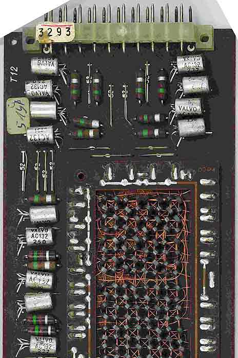
This is only a part of it to fit as integrated picture. See attachment.
What did I have to do with computers?
Guests which enter my home find a picture of a core memory board on the wall of the entrance hall. It is from my first computer which I could buy in 1972: a used IBM model 360-30, the first byte computer model (market introduction 1964). The memory was given to me for 20 years of "Data Center Luzern AG" by my staff in 1983. We got rid of the "old system" at that time, which served us so well. The rent of the system would have cost me 60 000 Swissfranks per month, so I have chosen to buy a used system - and found it in Philadelphia, USA. It was a hard job to insist that IBM Switzerland had to agree with a service contract or service it at all ...
Before we did use computers (like IBM 1401) from big companies at night by minute price which summed up to 25 000 Swissfranks a month. The memory board of IBM 360 has 16 KB and the machine had 4 of those boards. I tell this story just to show the difference to today. We needed a big, air-conditioned room and the system had a tiny fraction of "calculating power" compared with a todays netbook ...
I also tell this story because it was for one part "my own way" to handle things - 9 years hard work at night, then an outdated machine which even heated our business house I built in 1978 - and on the other hand the splendid staff (personnel) and the "old computer" which gave me the possibility to now finance Radiomuseum.org. I wondered then that the idea for using a computer as the only heating source seemed having been new ... We just filled two tanks with the warm water, the air-conditioning plant produced. Each tank does (still) hold 20 tons which only had to be distributed in the central heating which was in the ceilings. The building is well insulated and we could even de-ice a slope for cars outside the building.
Before I worked 5 years for IBM where I could save the money to start my own business. There I was first confronted with ferrite core memory. Before, in London, I was confronted with a tube computer at C.T. Bowring & Co. See the last link and open the documents from Christian Adam.
Some history about Ferrite Core Memory (Storage)
I don't know if the first ferrite core memory is based on US patent 2,667,542 (Electric Connecting Device) from Esmond Philip Goodwin Wright, London, England, assignor to ISE New York with priority GB September 26, 1950. It was filed Sept. 25, 1951 in the US. But Wright used only two wires - mainly for transferring communication currents by static coupling ... to co-ordinate switches for telecommunication switching systems.
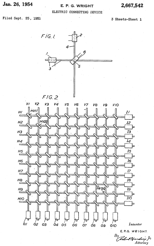
At least this started quite some work around this possibility to get rid of the Flip-Flop-Tube storages for the Central Processing Memory (CPU) with its ALU (Arithmetic Logic Unit, 1946 Neumann fro Princeton Institute of Advanced Studies (IAS) or later FPU (Floating Point Unit). This had to allow a non-cyclic or "random access", preferably keeping the memory when switched off. Before the ferrite core memory this had to be achieved either mechanically, by relais or by tubes entirely. Also magnetic drum storage devices and others were used partly for the "central memory" which stored certain programs, registers, variables, calculations, etc. but this could be a cyclic type.
Cyclic memories have to go through a complete cycle before a given element of information is available for reading, rewriting or alteration. There were used sonic or electromagnetic delay lines, magnetic drums and tapes, punched tapes and some forms of electrostatic storage tubes. Random Access Memories allow writing and reading within any part of the memory at any time. Before the ferrite core memory, banks of electromagnetic or electronic relays often made with cathode ray tubes (Williams-Kilburn tube) or "selectron" tubes were used.
Frederick W. Viehe (1947) and An Wang (1949) began independently experimenting with cores for computer memories - at about the same time vacuum tubes were replacing electromechanical calculators. Later development work was done by others, including the MIT, RCA and IBM. Jay Wright Forrester, working in MIT for the project Whirlwind, was perfecting the core memory and filed a patent May 11, 1951 which was patented Feb. 28, 1956 as 2'736'880. (Cited patents: 1504882, 2053156, 2430457, 2518022, 2519513, 2524154, 2574438 and 2696600).
The MIT memory is a matrix of magentic cores, supported by cross grids of wires, to which two pulses at the same time of electric current are applied to "address wires", one for a given column, the other for a given row. Selectors, first realized with tubes, drive the selection process. They are arranged at the outside of the actual matrix. This allowes to imply which core is addressed and at the same time feeds enough power to create a change - if the magnetic field is reverse. The third wire is the "sense wire" (or output wire) which detects changes of the magnetic field. It is an inhibit wire for each plane which threads all the cores in the plane. In the event of reading, two half cycles are used, one to detect a change (or not) and the second to re change again to the value before. To store or write one half cycle is enough. Each core represents a binary value of either 1 or Zero.
Just an example of such patents:
Milton Rosenberg (plus Modlinski, Oaks, Alexander, Palisades and Minka, assignors to Telemeter Magnetics, Inc.) filed March 28, 1955 a patent for a "Magnetic-Switch Cross-Coupling Minimization System". It was patented October 13, 1959 as 2,908,893. "Switching is achieved by selectively driving certain ones of a plurality of magnetic cores from saturation at one polarity to saturation at the opposite polarity by the use of vacuum tubes." They state: "Magnetic memories of the type employing arrays of magnetic cores having substantially rectangular hysteresis characteristics are presently finding favor as the memory components in information-handling machines. Such a memory is described in the article entitled "The M.I.T. Magnetic-Core Memory", by William N. Papian, published in the Proceedings of the Eastern Joint Computer Conference, Washington D.C, December 1953 (pages 37-42) ... In an article in the RCA Review, entitled "Static Magnetic Matrix Memory and Switching Circuits", by Jan A. Rajchman, volume 13, pp. 183-201, June 1952 issue, there is described a magnetic switch which may be employed to reduce the number of tubes required for driving the magnetic memory."
What we know is that IBM claims that it has used its flagship, the IBM 405 Alphabetical Accounting Machine (also called tabulator) from 1934 to build in an experimental core memory in 1952 - despite the fact that the machine was not sold anymore after May 1949 - except reconditioned machines (ibm.com). The system was tested in April 1952.
IBM used it then to replace the storage-tube memory in the IBM 701 Defensive Calculator, IBM's first commercial scientific computer and at the same time first large-scale computer and first IBM machine with programs stored in an internal adressable electronic memory. The storage were 72 Williams tubes with a capacity fo 1024 bytes each. The memory cycle time for both, Williams tube or later magnetic core was 12 microseconds. First appereance on market April 7, 1953. 19 systems sold.
In the early 1950ies there were quite some articles about ferrite core memories like J.W. Forrester in an article entitled "Digital Information Storage in Three Dimensions Using Magnetic Cores" in the Journal of Applied Physics volume 22, page 44 of January 1951. Or David R. Brown and Ernest Albers-Schoenberg with "Ferrites Speed Digital Computers" in "Electronics" page 146 of April 1953, published by the McGraw-Hill Publishing Company. Or N. Pappian in an article on page 194 of the same Journal, March 1955 for a ferrite core memory using pulse transformers, arranged in separate planes, with each plane having for example 64 horizontal and 64 vertical rows of cores, resulting in a total of 4096 cores per plane.
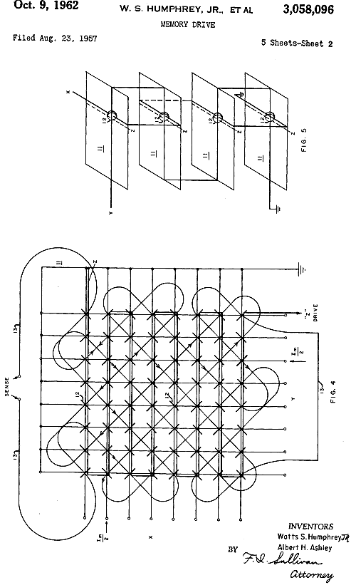
Many patents then dealt with the high number of vacuum tubes required as coordinate drivers (3,058,096 Watts S. Humphrey, Cochituate and Albert H. Ashley for Sylvania Electric Products Inc., filed Aug. 23, 1957), the speed, the problem of disturbances (Bauer 2,889,540, filed July 14, 1954 - with tubes like for Russell in 2,929,050, filed May 27, 1955) etc. and the techniques for being able to get away from the hand made process and later to solid state technique and to printed circuits like the one above. The first patent about ferrite core memory on printed circuit is probably Paul V. Horton for IBM, filed May 10, 1955, patented Jan 31, 1961 as 2,970,296.
Just to show a fraction of patents I list here the cited patents in the 2,970,296. It is listed by patent date, not filing date which can be even years earlier:
1,988,734 Helgason, Jan. 22, 1935
2,588,726 Hoover, Mar. 11, 1952
2,603,681 Salisbury, July 15, 1952
2,654,142 Horelick, Oct. 6, 1953
2,700,150 Wales, Jan. 18, 1955
2,712,126 Rosenberg et al. June 28, 1955
2,719,965 Person, Oct. 4, 1955
2,724,103 Ashenhurst, Nov. 15, 1955
2,732,542 Minnick, Jan. 24, 1956
2,734,150 Beck, Feb. 7, 1956
2,757,443 Steigerwalt et al., Aug. 7, 1956
2,762,113 Daniels et al., Sept. 11, 1956
2,774,014 Henry, Dec. 11, 1956
2,784,391 Rajchman, Mar. 5, 1957 (see also Rajchman 2,691,154)
2,792,563 Rajchman, May 14, 1957
2,823,371 Jones, Feb. 11, 1958
2,870,433 Simpson, Jan. 20, 1959
Roughly about 10 years before the appeareance of IBM 360-30 or the board above with the AC132, transistors were used. In the IBM 1401 from October 1959 they have been packed into common housings for a half a dozen transistors in the same case and for the IBM 360 brought more integration with Solid Logic Technology (SLT) but VLSI with thousands of transistor-based circuits began in the 1970s when complex semiconductor and communication technologies were being developed. The microprocessor is an example but now it integrates hundred of millions of transistors.
A model page for Ferrite Core Memories
To be able to show early and later examples of Ferrite Core Memories I have introduced a model page to Radiomuseum.org. Please use the link above the text. I have none of such Magnetic Core Memories with tubes and hope somebody has and can upload photos - or finds images in the literature. Anyway it is clear that tubes were involved at the start which gives us the reason to introduce also Ferrite Core Memories - but we will not create more model pages but use this one for presenting more articles and/or pictures. We can remember: The development of transistors (Translation from Vincent de Franco) and of the ferrite core memory was about at the same time.
To thank the Author because you find the post helpful or well done.
The way Wikipedia tells the history of Magnetic Core Memory
After writing my text I was corious what Wikipedia.org shows as history. I did not want to see it before, because I would have been influenced. Here Wikipedia as a quote:
"The earliest work on core memory was carried out by the Shanghai-born American physicists, An Wang and Way-Dong Woo, who created the pulse transfer controlling device in 1949. The name referred to the way that the magnetic field of the cores could be used to control the switching of current in electro-mechanical systems. Wang and Woo were working at Harvard University's Computation Laboratory at the time, but unlike MIT, Harvard was not interested in promoting inventions created in their labs. Instead Wang was able to patent the system on his own while Woo took ill.
Jay Forrester's group, working on the Whirlwind project at MIT, became aware of this work. This machine required a fast memory system for realtime flight simulator use. At first, Williams tubes (more accurately, Williams-Kilburn tubes) — a storage system based on cathode ray tubes — were used, but these devices were always temperamental and unreliable.
Two key inventions led to the development of magnetic core memory in 1951, which enabled the development of computers as we know them. The first, An Wang's, was the write-after-read cycle, which solved the puzzle of how to use a storage medium in which the act of reading was also an act of erasure. The second, Jay Forrester's, was the coincident-current system, which enabled a small number of wires to control a large number of cores (see Description section below for details).
Forrester's coincident-current system required one of the wires to be run at 45 degrees to the cores, which proved impossible to wire by machine, so that core arrays had to be assembled by workers with fine motor control under microscopes. Initially, garment workers were used.
It was during the early 50s that Seeburg developed the use of this coincident current ferrite core memory storage in the 'Tormat' memory of its new range of jukeboxes, starting with the V200 released in 1955. Development work was completed in 1953.
By the late 1950s industrial plants had been set up in the Far East to build core. Inside, hundreds of workers strung cores for low pay. This lowered the cost of core to the point where it became largely universal as main memory by the early 1960s, replacing both the low-cost and low-performance drum memory as well as the high-cost and high-performance systems using vacuum tubes, later transistors, as memory. Certain manufacturers also employed Scandinavian seamstresses who had been laid off due to mechanization of the textile industry.
The cost of core memory declined sharply over the lifetime of the technology: costs began at roughly US$1.00 per bit and eventually approached roughly US$0.01 per bit. Core was in turn replaced by integrated silicon RAM chips in the 1970s.
Dr. Wang's patent was not granted until 1955, and by that time core was already in use. This started a long series of lawsuits, which eventually ended when IBM paid Wang several million dollars to buy the patent outright. Wang used the funds to greatly increase the size of Wang Laboratories which he co-founded with Dr. Ge-Yao Chu, a school mate from China."
I add from Wikipedia something about physical characteristics for a better understanding about the pro's and contra's of usage and the understanding of function and problems:
"Physical characteristics
The performance of early core memories can be characterized in today's terms as being very roughly comparable to a clock rate of 1 MHz (equivalent to early 1980s home computers, like the Apple II and Commodore 64). Early core memory systems had cycle times of about 6 µs, which had fallen to 1.2 µs by the early 1970s, and by the mid-70s it was down to 600 ns (0.6 µs). Everything possible was done in order to increase access, including the simultaneous use of multiple grids of core, each storing one bit of a data word. For instance a machine might use 32 grids of core with a single bit of the 32-bit word in each one, and the controller could access the entire 32-bit word in a single read/write cycle.
Core memory is non-volatile storage – it can retain its contents indefinitely without power. It is also relatively unaffected by EMP and radiation. These were important advantages for some applications like first generation industrial programmable controllers, military installations and vehicles like fighter aircraft, as well as spacecraft, and led to core being used for a number of years after availability of semiconductor MOS memory (see also MOSFET). For example, the Space Shuttle flight computers initially used core memory, which preserved the contents of memory even through the Challenger's explosion and subsequent plunge into the sea in 1986.
A characteristic of core was that it is current-based, not voltage-based. The "half select current" was typically about 400 mA for later, smaller, faster cores. Earlier, larger cores required more current.
Another characteristic of core is that the hysteresis loop was temperature sensitive, the proper half select current at one temperature is not the proper half select current at another temperature. So the memory controllers would include temperature sensors (typically a thermistor) to adjust the current levels correctly for temperature changes. An example of this is the core memory used by Digital Equipment Corporation for their PDP-1 computer; this strategy continued through all of the follow-on core memory systems built by DEC for their PDP line of air-cooled computers. Another method of handling the temperature sensitivity was to enclose the magnetic core "stack" in a temperature controlled oven. Examples of this are the heated air core memory of the IBM 1620 (which could take up to 30 minutes to reach operating temperature, about 106 °F, 41 °C) and the heated oil bath core memory of the IBM 709, IBM 7090, and IBM 7030."
Remark:
You may copy text from Wikipedia since it is in public domain, financed by the public under the condition: "as long as the use is attributed and the same freedom to re-use and re-distribute applies to any derivative works."
To thank the Author because you find the post helpful or well done.
Core Memory
Hello,
The first computer I programmed, a long time ago, had a magnetic core memory, a mid 1960s British built ICL 1906S....
A group of enthusiasts here in the UK are currently restoring an early core memory machine back into full working order, a 1962 British built ICT 1301. That is some restoration project !
http://www.ict1301.co.uk/13010110.htm
http://en.wikipedia.org/wiki/ICT_1301
Regards ......... Howard
To thank the Author because you find the post helpful or well done.
Very early ferrite memory stack
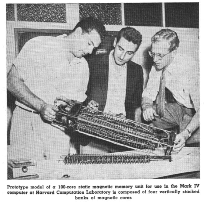
Electronics, January 1951 talks of the prototype of one of the early static magnetic core memory, built by Marshall Kincaid, from Harvard Computation Laboratory, together with John M. Alden and Robert B. Hanna, from Alden Products Co. This work was derived from preliminary studies on the possible applications of magnetic materials showing rectangular hysteresis loops. These materials, such as the Deltamax from Allegheny Ludlum Steels Corp, were the US outgrowth of the Permanorm 5000Z, discovered by German scientists during WWII. According to the article, Horward Aiken of the Harward Computation Laboratory foresaw the possible use of these materials to store information and its idea was carried out in the next two years by An Wang and Way Dong Woo.
The prototype was a magnetic memory containing 100 cores (100 bits), assembled in four stacked banks of 25 cores each, which was used as buffer of a 23 bit by 23 bit multiplier inside the Mark-VI computer of the same University. Each core was similar to a ferrite pot core with diameter of about 20mm. Maximum clock speed was limited to 30,000 pulse per second (30KHz).
Also a 8-bit shift register was built with the same cores. This unit was used to convert parallel to serial data or vice-versa. The article also describes the use of ten cores subassemblies in a counter/prescaler.
Readers can refer to pages from 108 to 111 of Electronics, January 1951. Here the pictures from the article.
Of course, I have no direct experience of these early applications that were however fascinating, since core memories were in use until the late seventies, and even later if we consider the magnetic bubble memories as their evolution. What I want to underline is how little memory space was used before the introduction of semiconductor memories. Around 1970 I, still student, was regularly called to service the computer of the Polytechnic of Naples, a Control Data G-20, for which I designed and built replacement boards and peripherals, such as the modem interface. Well this monster came with 8KBytes core memory factory installed. A second 12KB module, made by Mullard, had been added: this module alone was a rack unit higher than 2 meters.
In the same years a complex flight computer could have as low as 4 Kwords of memory space to store everything, from programs, including self-test routines, reckoning and course computation, to data, including data of stars used for astronomic navigation. Sometimes I say to myself that with such a little memory space men went to the Moon and I wonder why computers today waste GBytes or TBytes of memory.
Nevertheless it could be nice if some German members can add more about the applications of Permanorm 5000Z, if any.
Best regards, Emilio
To thank the Author because you find the post helpful or well done.
Memory
Friend Ernst,
After reading your article I didn't resist in of putting here this it announces that it almost came in all from the daily newspapers, the following day to the disembarkation.

http://www-03.ibm.com/ibm/history/exhibits/storage/storage_PH0305.html
Cordially
Júlio Branco
To thank the Author because you find the post helpful or well done.
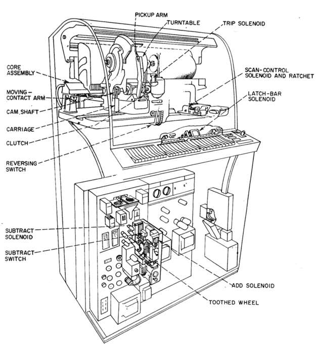
Juke box uses ferrite-core memory
The use of ferrite-core memory in the record selection system of a juke box was first suggested in 1953, to replace solenoid-actuated selection levers. The design of the new selection system required about two years and the first commercial application appeared in 1955, in the Seeburg Select-O-Matic 200 model. This new application was first announced in Electronics, June 1955 and a detailed article appeared in the October 1955 issue of the same magazine..jpg)
The 200 ferrite-core memory array was electrically organized as 10 rows by 20 columns. Cores were physically arranged in two rows, 100 cores each, parallel to the player carriage rail: one row was associated to side A of the records, the remaining to side B. The selection of records, enabled by a credit toothed wheel after having inserted coins, was performed pushing both a letter (column) and a number (row) keys. A write capacitor was discharged, magnetizing the core at the intersection of the two matrix wires selected by the pushbutton keys. The credit on the toothed wheel was then decreased and the circuit was ready for a new selection, until zero credit was reached.
Memory matrix
Physical arrangement
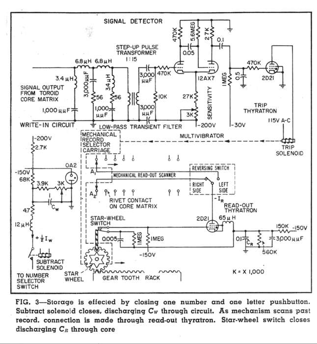
The play sequence started moving the turntable carriage, and an associated contact arm, first from extreme right position to left and then in the opposite direction. A brush on the contact arm touched in sequence a riveted electrical contact at each core. Reading was performed discharging a capacitor through a 2D21 thyratron. 40 seconds were needed to scan all the 200 cores. Magnetized cores returned an output signal pulse on the sense wire. This signal was used to temporarily stop the carriage advance and to start the reproduction sequence of the selected record. At the end of the record reproduction, the core scan was resumed until the end of the memory array was reached.
Store/Read circuit
To avoid expensive rewiring, each core was individually tested before assembling operations. A final 2.5 minutes test was carried over the complete ferrite-core matrix assembly, performing a write-in and a successive read-out cycle for each core.
To thank the Author because you find the post helpful or well done.
Ferrite-core Memories around the mid '950s.
Starting from the early 200-bit ferrite memory described above, within few years the improvements in circuits and in core materials gave larger and faster memory arrays, readily transferred from research laboratories to commercial computers. The development of ferrite memory arrays coincided with the migration of computers to solid state. The miniaturization and the power savings coming from using transistors made possible the design of high-speed, high-performance computers. Therefore the demand for larger and faster internal memories went up. Ferrite arrays proved fast enough to replace CRT memories and other systems, with considerable advantages in terms of reliability and volume per bit. Early in 1955, top computer manufacturers had announced or in production at least one machine, using more or less semiconductors and ferrite memory banks. IBM had announced its solid-state 608, for delivery early in 1956; but also IBM 705, Raytheon Raycom, RCA Bizmac and Remington Univac II were equipped with high-speed ferrite core memories; see also ‘1955 computer survey in US’. The Lincoln Laboratory of MIT was one of the pioneers in the design of large arrays.
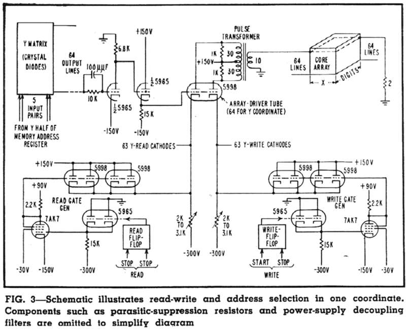
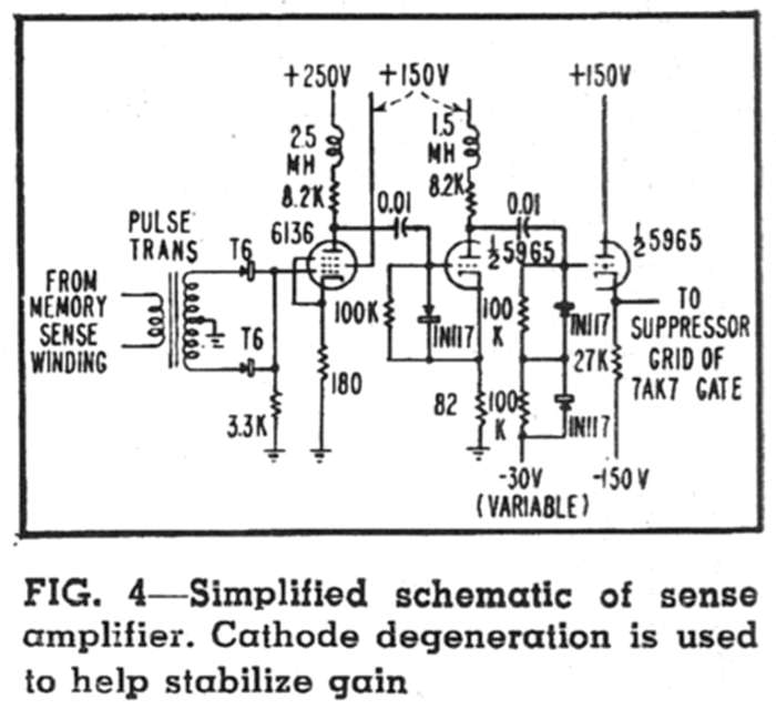
William N. Papian in Electronics, March 1955, describes the new fast ferrite-core memory, a 64 x 64 array or 4096 registers, each 17 bit long. Each memory plane was a square array with 64 x and 64 y address lines. Ferrite doughnuts measured only 80 mils in outside diameter.


Address selection circuits included crystal diode decoders and vacuum tube buffer-drivers. 5998 twin triodes, high-gain variants of 6AS7, were used as drivers. Each one of the 17 sense amplifiers included a 1:5 step-up balanced linear transformer, which raised the pulse level to about 0.5V, and a three stage amplifier, so reaching about 30V to drive the 7AK7 gate tubes. See also the use of the vacuum tube 5965 in the first link below (picture).
Address and R/W simplified diagram
Sense amplifiers simplified diagram
The memory assembly, shown in the following picture, actually included 19 planes, two being reserved as spares. 635 vacuum tubes were used in this unit.

In October 1957 the same author, William N. Papian, described in Electronics the new high-speed ferrite-core memory array designed for the Lincoln TX-2 high-performance computer. 
TX-2 computer overview with the large memory at left behind the console.
The new 2.5-megabit array was organized in two banks. The first one with 256 by 256, or 65 kilowords, 36-bit each word, plus a parity and a spare bits. The second bank had 4096 words of the same length. Further banks could be added, up to a total of 262 kilowords or about ten million bits. Banks could be operated independently and simultaneously. The big memory operated with 6 microseconds total cycle time at 5MHz clock frequency. Cores, made and tested at Lincoln Laboratory, measured just 80 mils (2 mm) outside diameter by 20 mils (0.5 mm) high each. About 22,000 transistors, several hundred diodes and 625 vacuum tubes were used in this memory. 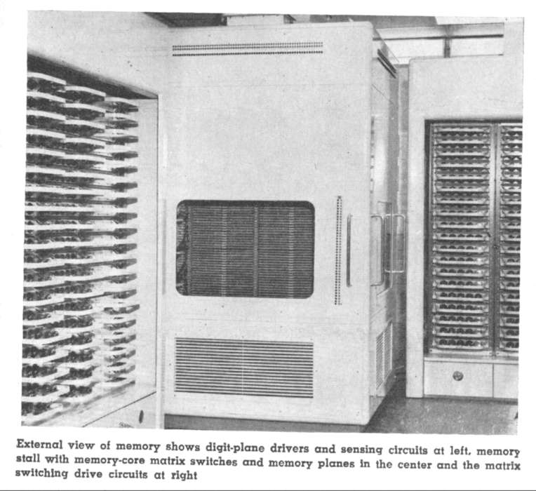
From left: Digit-plane drivers and sensing circuits unit, memory planes with matrix switches unit and matrix switching drive unit at right.
An additional fast access storage unit was used for the manipulation of sixty-four 19-bit registers, used to store indexed addresses or program counters. The access time for this module was just 0.6 microsecond, the full cycle requiring 4 microsecond. The module required a total of 434 transistors, 8 diodes and 1 vacuum tube.


View of the high-speed 64 x 19 memory unit, containing the sense and drive boards mounted upside-down. A close-up view of the ferrite cores is also given.
To thank the Author because you find the post helpful or well done.
Sigle bit core module
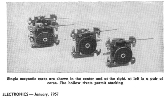
In Electronics, February 1951, Alden Products Co. advertised its model 5100RA single core memory module, used as basic building block for the 100 bit memory array just built at the Harvard Computation Laboratory. See 'Very early ferrite memory stack above'.
.jpg)
To thank the Author because you find the post helpful or well done.
Related book

Thank you Emilio and Ernst for your excellent presentations.
My friend Doug Coulter, who works on nuclear fusion, has suggested this open source google-book as an interesting snapshot of pulse oriented design technique in the mid 1950's.
Multi channel Pulse Height Analyzer
The book was published by "National Research Council (U.S.). Committee on Nuclear Science"
If this link does not work, enter "Multi channel Pulse Height Analyzer" in Google-books.
This book scan has 219 pages. The general topic of the book is the proceedings, or better, the minutes, of an informal conference surveying pulse height analysers that measure the pulses from nuclear radiation detectors.
The circuit types include very early tube-based analog-to-Digital converters, pulse shaping networks, voltage comparators, which were then named "discriminators", and many delay and memory circuits with delay lines, storage tubes, and core memory.
Memory was a very important part of these designs because the measuring method for the nuclear radiation is based on collecting histograms of pulse height.
Regards,
-Joe
To thank the Author because you find the post helpful or well done.
Ferrite Core Memory - some History
This is a picture of a LEO Computer core board which may be a boot code given the torroids only present on some junctions.
Any further information appreciated.
John Hansen
Attachments:- LEO CORE BOARD (28 KB)
- DSCF0003_RM_RES (28 KB)
To thank the Author because you find the post helpful or well done.