The operational amplifier made simple
The operational amplifier made simple

Foreword:
In the past simple analog circuits were used to solve many problems of measurement, control, signal processing, data acquisition and interface to digital computers. Operational amplifiers were the ideal building blocks for designers to quickly reach reliable and predictable solutions, their precision and stability just depending upon a few external components, mostly resistors and voltage references, readily available. Every kind of circuit could be readily made around them: amplifiers, comparators, filters, oscillators, integrators, current pumps, level translators and much more, everything a designer could need in the era of analog computers.
The operational amplifier or op-amp is a gain structure with two differential inputs, the non-inverting and the inverting ones, and one output. The early tube op-amps were marketed in the early 1950s by George A. Philbrick Research of Boston, US. In the following photo one early amplifier, with octal base. Modern op-amps are very similar for number of pins and functionality to that ones.
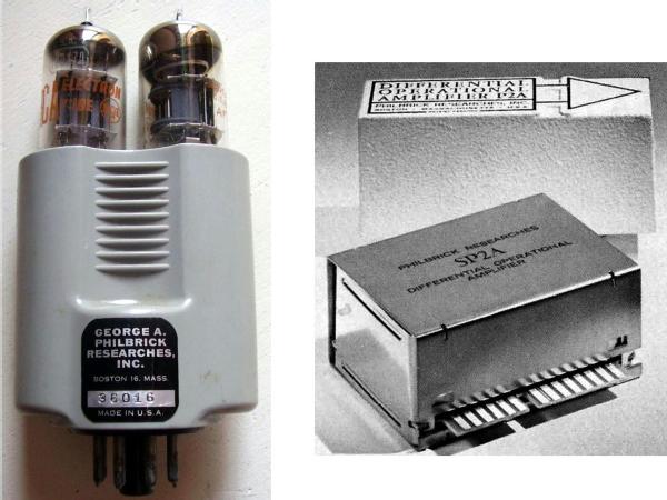
Fig. 1 - Left, Philbrick K2-XA high-gain operational amplifier. Amplification greater than 30,000 was specified, with output voltage swing greater than ± 100 V. Right, early transistorized amplifiers P2A and SP2A, 1962. Click on the image to enlarge.
Early tube operational amplifiers evolved in the years, first in the form of transistorized circuitries put in metal cases or in molded blocks, then in monolithic circuits, among which the most popular became the 741. In monolithic op-amps there are just two pins for power which can be connected to a bipolar supply, for example ±15 Volt, or even to a single supply, for example +12V. There is no ground pin, i.e. no pin connected to the zero or center point of the power supply. Then the common questions are: how do I connect a signal source to the input? And again, what voltage will I read at the output in the absence of any input signal?
The voltage gain of any op-amp is very high, in the order of tens or hundreds of output volts per millivolt in input. The swing of the output voltage covers the entire power supply range, except for modest drops in the junctions of the output stage. Due to its high open-loop gain an op-amp can be used as comparator. If the non-inverting input moves to a voltage even slightly higher than that at the inverting input, the output will go to a value close to +Vcc. As soon as the voltage polarity on inputs reverses almost suddenly the output moves close to -Vcc. If we try to use a similar comparator, we realize that there is an uncertainty band, corresponding to voltage difference under approximately 100 microvolts between the two inputs, in which the circuit behaves in a linear way, with its output voltage somewhere between +Vcc and -Vcc. This happens because the difference of the two signals multiplied for the open-loop gain is not enough to saturate the output stage and our op-amp is working in its linear region. In any case, since inputs are differential, the comparator will work for any pair of input voltages, as long as within the specified allowable voltage range.
Such a comparator, due to the high gain typical of an operational, will be very sensitive. Therefore it can compare voltages differing from each other by millivolts or fractions of millivolts. It will be necessary to add positive reaction with some hysteresis to prevent unpredictable levels and also oscillations when inputs of our op-amp are at very similar voltages.
Observations made about the operational used without feedback as comparator allow us to easily understand how the output does not depend upon the absolute value of the two inputs but rather on their relative values, or in other words on the voltage difference between them. Output signal is free then to move linearly between the two supplies, negative and positive. So far there is no need for a common ground point, except when interfacing ground referred signal sources and/or output loads.
Typical open-loop gain of a 741 op-amp is greater than 50V/mV: then a signal difference of fractions of millivolts in input would drive the output stage to saturation. We need to introduce a negative feedback, as in the circuits below, with signal to the non inverting or to the inverting input:
 |
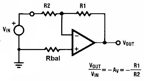 |
Fig. 2 - At the left the typical diagram of non-inverting amplifier, at the right an inverting amplifier. In the first circuit the signal Vin sees near to infinite impedance. In the second circuit the input impedance is R2, since the node between R1 and R2 is a virtual ground.
In the first circuit, the signal is applied to the non-inverting input and the inverting input moves to the fraction of the output signal present on the divider R1 / R2. In the second circuit, the Vin signal is applied to the inverting input and adds algebraically to the feedback voltage, so as to always drive this input to the potential present on the non-inverting input. In other words, the node between R2 and R1 constitutes a virtual ground, which can be used to add several signals together, as in the circuit in fig. 3. Note that currents, the ones coming from external signal on the left and the one coming from the output voltage through the feedback resistor, sum algebraically in the In- node, so to force its voltage to the same value of In+, in this case ground. All the currents flow according to the arrows, none flowing in the inverting input pin. Actually in bipolar op-amps small currents flow in the two input pins. We are neglecting them since in this case, due to high gain of the amplifier, they are much lower than the ones indicated by the arrows. These currents, in the order of a few tens or hundreds of nanoampere, are defined input bias currents or Ib.
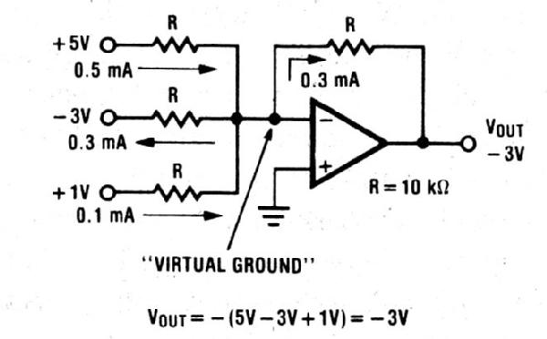
Fig. 3 - A virtual ground is present where currents from external sources algebraically sum to the current from the output through the feedback resistor. C,ick on image to enlarge,
Operational amplifiers have been offered in a variety of models, characterized by different performances, also including hybrid ones to accurately trim some parameters. Important parameters to consider when selecting the proper op-amp are the voltage gain, Av, the gain bandwidth product (GBW), plus the said input bias current, the input offset voltage and their respective thermal drifts.
The voltage gain Av, always referred to the open-loop configuration, is the ratio between a change in output voltage and the corresponding small change in the input differential voltage. It is commonly expressed in V / mV. Typical values are in the order of 100.000 V/mV or higher.
The gain of any amplifier decreases as the frequency of the signal increases. The gain bandwidth product, GBW, is the frequency at which the open loop gain reaches the unity. It is expressed in Hz.
By definition the input bias current is the average current in the inputs with the output at the center of its swing. Circulating in the resistors connected to the inputs, bias currents generate small voltage offsets which sum algebraically to signals and to DC biasing voltages. In the circuit shown above, the non-inverting input pin is connected directly to ground. To prevent any unbalance due to the Ibias flowing in the equivalent resistance connected to the inverting pin, a resistor of the same value should be added between the non-inverting input and ground.
The input offset voltage indicates the voltage that should be applied between the two inputs in order to set the output at the center of its range. It could be expressed in µV or in mV.
Incidentally, the ground generally coincides with the central point of a bipolar power supply, for example ± 5V, ± 12V or ± 15V. Anyway, whenever a single supply is available, our DC reference may be obtained by means of a resistive divider or rather a zener diode or even a voltage regulator. Of course our DC reference may be asymmetric, moved toward one of the supply ends.

Fig. 4 - Two simple ways to split a single supply in two, to create the reference to which refer the non inverting input of the op-amp, so setting its the quiescent DC output level.
Sometimes, as in the case of sensing the unbalance of a measurement bridge, we may need high impedance at both inputs. Then we can use the ‘instrumentation amplifier’ shown below. Each input goes to non inverting pin of the two op-amps A1 and A2. The third op-amp A3 sums the outputs of the first two gain cells through a resistor network. This arrangement gives very high input impedances, both at the non inverting and at the inverting input. The overall gain of the instrumentation amplifier below is 100. The gain can be increased or adjusted, replacing R3 with a resistor of lower value in series with a variable resistor. Resistor pairs R2/R5 and R6/R7 must be carefully matched for high CMRR or common mode rejection ratio.
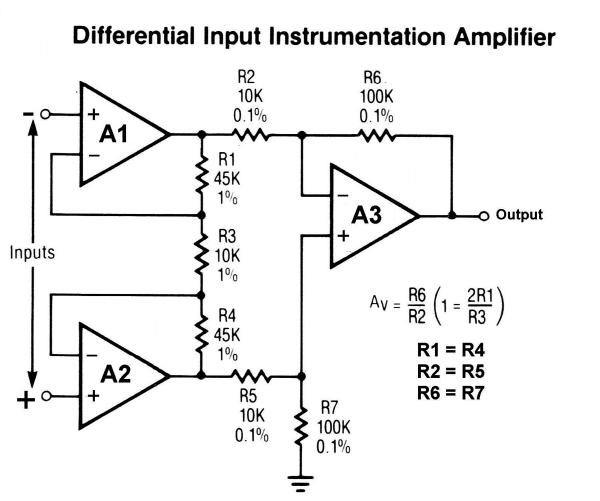
Fig. 5 - High impedance differential input instrumentation amplifier. Click to enlarge
Many useful application circuits can be found in the data sheets of common op-amps. A handy guide for designers and experimenters was ‘Intuitive IC Op-Amps’ by Thomas M. Frederiksen.
To thank the Author because you find the post helpful or well done.
Philbrick OpAmp additional Information

Additional information on the Philbrick operational amplifier, including its schematic, will be found at:
To thank the Author because you find the post helpful or well done.
Useful application circuits
The prehistory of the analog electronic computing, up to the wartime evolutions were fully summarized in the Achim Dassow's post. Before moving to applications of op-amps, here is just a quick note about the postwar evolution of vacuum tube analog computers which originated op-amps modules as well as the many sensors, actuators and modular interface and computing circuitries.
Electronic analog computers evolved into the RCA Typhoon, which in the early fifties made it possible to simulate on a large plotter the interception trajectory of a missile toward its target. Impressive details and photos of that amazing computer were given from February 1951 in several issues of Electronics. Here the front cover of Electronics, April 1951 with shelves full of electronic control panels around the plotter simulating the interception (click on image to enlarge):

Electronic analog computing was widely used well into the sixties for any kind of applications, attitude controllers, fire control systems, navigation systems, industrial controls and instrumentation up to large computers used in design centers to simulate the behavior of ships, missiles, planes, power plants as well as complex physical phenomena. Whatever the complexity of any analog computer was, it was capable of processing all input variables continuously and simultaneously, while driving all outputs at the same time. Around 1970, with the spread of integrated circuits, logic families and MOS memories, size of digital computers rapidly decreased, while their performance increased. The drawback was that CPU could handle just one signal at a time. They were too slow, since data had to be processed sequentially. For a while hybrid computers were tried, with digital computers controlling analog ones. I myself designed and built the interface equipment to connect an HP 2100 mini to a Hitachi 505 analog computer, when the Study Center for Hybrid Calculators was established at the Polytechnic of Naples in 1973. Most of the circuitries developed for analog computing were later integrated as modular interfaces for digital computers.
Transition to modular amplifiers and to solid-state solutions, up to the borderline between PCB or hybrid modules and fully integrated circuits, is exceptionally documented today in the site dedicated to the history of the George Philbrick Research, thanks to Prof. Joe Sousa who patiently collected lots of documents, notes and witnesses from the same people which designed op-amps. philbrickarchive.org.
Coming to the applications of our op-amps, below readers can find a selection of simple yet useful circuits given in the databooks of leading IC manufacturers.
Simple application circuits (click on each image to enlarge)
 |
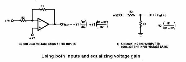 |
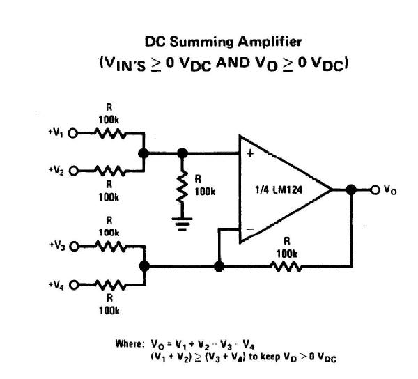
Left: Generalized summing amplifier. Inputs can be expanded and AC signals can be superimposed to some of them, when required. - Right: How to use both inputs to sum two signals. The same circuit, with voltage divider on the non-inverting input connected between Vs+ and Vs-, is normally used to set the quiescent DC output voltage of the op-amp.
Current sensors and current generators
 |
 |
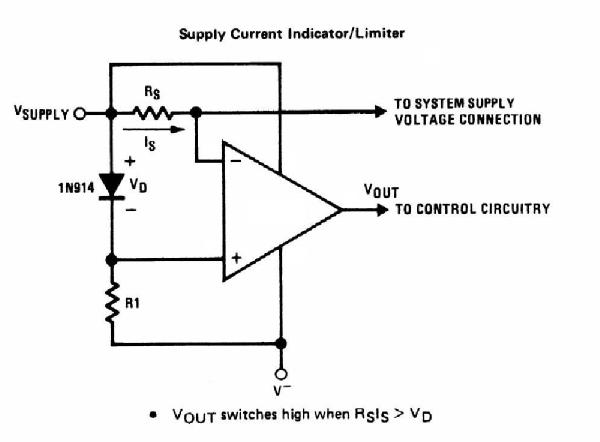
Left: The op-amp senses the current of a power supply flowing in Rs: when the voltage drop across Rs exceeds the forward voltage of the 1N914 silicon diode, the op-amp output sends a high level to the external control circuit. - Right: The voltage drop across Re must be the same as Vref across R1, so fixing the current flow in Re and hence in the transistor emitter. Using high beta transistor, the collector current can be assumed to be quite the same, just differing for the little base current. A zener or a compensated zener diode could be used for Vref.
 |
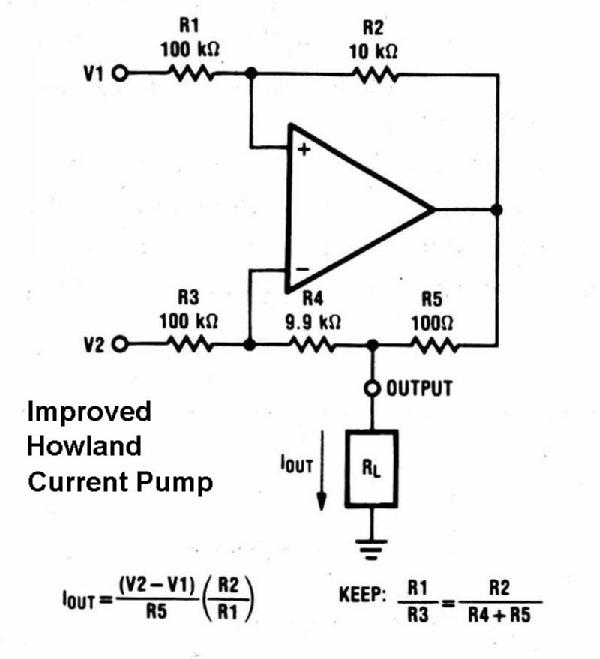 |
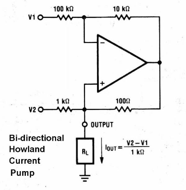
Current pumps are bidirectional current generators. Left: The basic Howland current pump. V1 input can be grounded and then Iout is controlled only by V2. - Right: This improved circuit offers better insulation between V2 and R1 and limits the op-amp current drive.
Active filters
 |
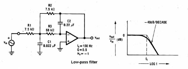 |
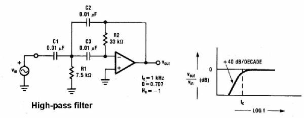
Active filters were widely used to extract even the weakest signals from background noise. Typical circuits for high-pass and low-pass active filters.
 |
 |
Two band-pass active filters. Q of the first one, an infinite gain, multiple feedback type, is 5. - Two gain cells must be used, as in the second circuit, if higher Q is required, 25 in this case
 |
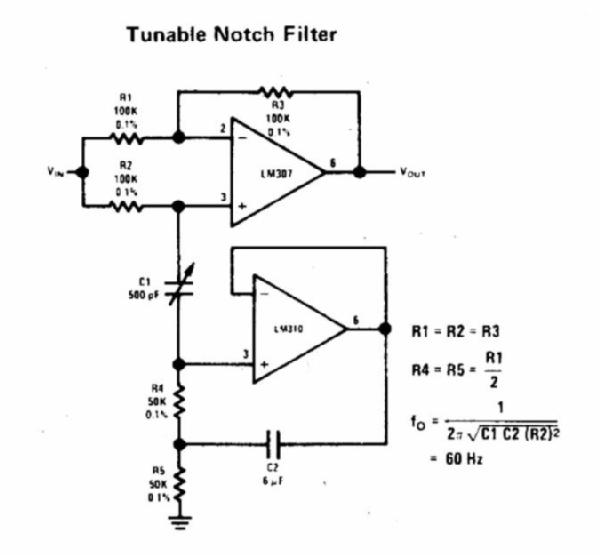 |
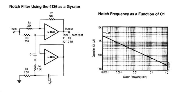
Notch filters were commonly used to cut noise generated at a given frequency, such as hum noise at the mains frequency, 50 or 60 Hz. Here are two of them with design data.
AC amplifying and measuring circuits
 |
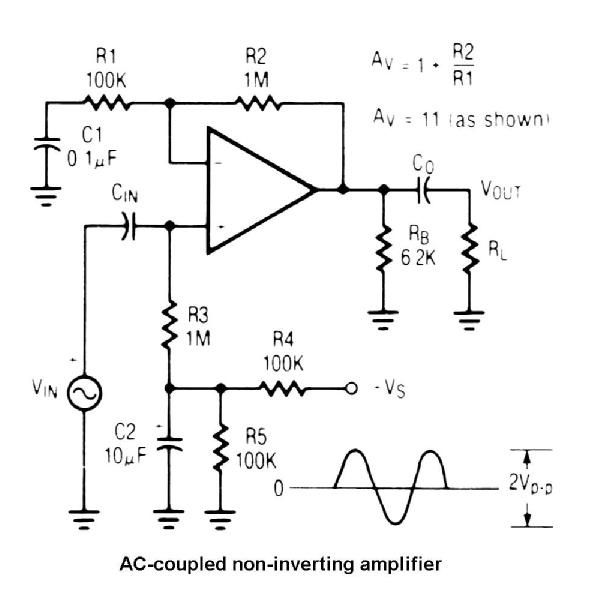 |
Two AC-coupled amplifiers using op-amps. In the first one the divider R2 / R3 sets the DC level of the output stage. In the second one the DC level is set by the voltage divider R4 / R5, with R3 and C1 used to decouple the AC input signal from the DC biasing path.
 |
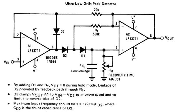 |
Left: An absolute value rectifier used in many multimeters to measure AC voltage. - Right: Peak detector using a very smart solution to minimize leakage paths for the capacitor. Resistor Rf biases the anode of D1 at the same voltage existing at the cathode node: since the voltage across D1 is zero, no current can flow in it. Apart from the input bias current of A2, 100 pA worst case, the capacitor discharge is fully predictable, across the ‘recovery time adjust’ trimmer.
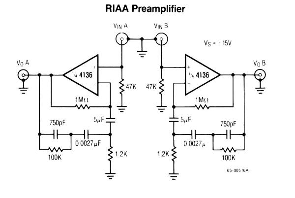 |
 |
Some op-amps were intended for audio applications. They were designed for high slew rate and mainly for very low noise. Left: RIAA equalized preamplifier for phono pick-up cartridges. - Right: The same low-noise op-amp can be used for this stereo tone control.
Oscillators and more...
 |
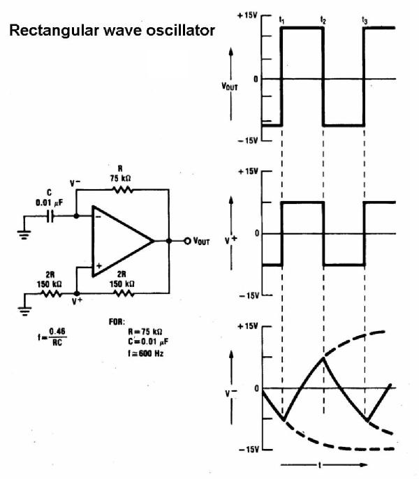 |
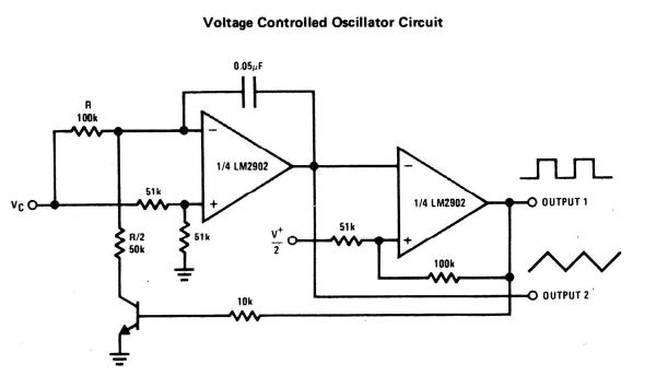
Left: Voltage controlled oscillator, VCO, is useful to convert a variable signal into a variable frequency which could be transmitted over a twisted pair or even via radio, to be read somewhere else. The first op-amp is used as integrator and the second amplifier acts as a comparator, discharging the capacitor by means of a transistor. - Right: Rectangular wave oscillator. A signal approximating a triangular wave can be picked up, connecting a high-input impedance buffer to the integrating capacitor C.
 |
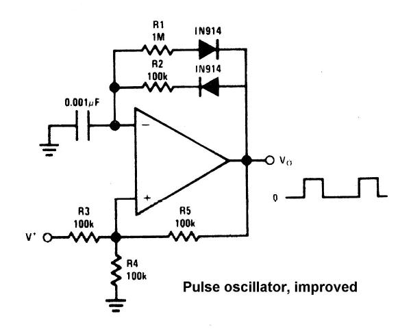 |
Left: In this oscillator high output state charges the capacitor through R1, then the diode becomes reverse biased and the capacitor discharges through R2. - Right: In this case there are two separate paths for charging and discharging the timing capacitor, each path activated by the conduction of corresponding diode. Pulses very short or very long compared with the total p.r.r can be easily generated.
 |
 |
Two sine wave oscillators. The first one uses zener diodes in the feedback loop to control the amplitude. It generates both sine and cosine outputs. In the second oscillator a lamp is used as PTC, to control amplitude.
 |
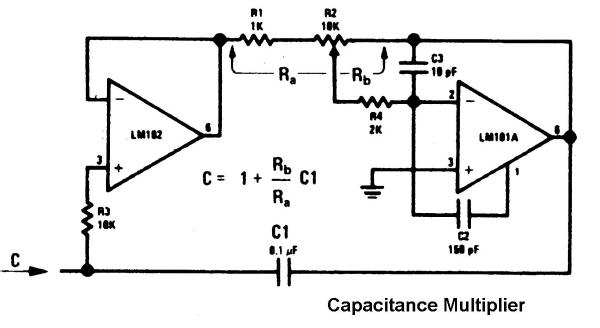 |
Here two amazing examples of what op-amps could do. In the first circuit a capacitor is used to simulate an inductor. I myself used this circuit to build an LC resonant circuit based upon two capacitors. The second circuit is a capacitance multiplier. Think about the possibility of creating a tunable resonant circuit using two capacitors and a potentiometer!
Diagrams shown above were taken from:
- Thomas M. Frederiksen, Intuitive IC Op Amps, 1984
- National Semiconductor, Linear Databook 1982
- Raytheon, Linear Integrated Circuits
To thank the Author because you find the post helpful or well done.