Tuned power supplies in the '30s
Tuned power supplies in the '30s

One of the technical and economic problems in designing AC-powered radio sets at the beginning of the ‘30s, concerned the sizing of high voltage capacitors in the power supply that, before the introduction of electrolytic types, were bulky and expensive paper capacitors that made impractical the use of a total capacitance larger than, say, 6-10 µF.
The standard design can be considered that reported in Figure 1 where the inductor is the field coil of the electrodynamic loudspeaker; the typical design included, usually, also a resistor to create the negative grid polarization voltage for the output power tube but it has been omitted in Figure 1 because its presence is not relevant in the context of this discussion.
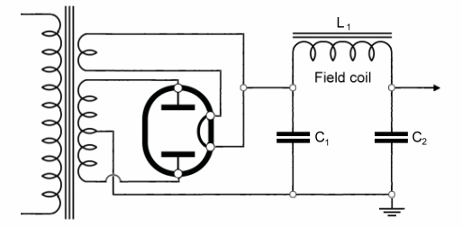
Figure 1 - Typical power supply in AC receivers
The problem is, of course, achieving an acceptable hum level and, to this purpose, some creative solutions have been introduced (see, for instance, the hum-bucking coil described in the outstanding paper The development of the loudspeaker by Prof. Dietmar Rudolph). Another clever and intriguing solution can be observed in some receivers that adopted a more sophisticated power supply design requiring an additional inductor and an additional, comparatively small, capacitor; the typical circuit is reported in Figure 2

Figure 2 – Tuned power supply
I have used the term “tuned” to distinguish this kind of power supply from standard designs and also because the parallel of L1 and C3 constitutes a resonant circuit whose influence cannot be directly evaluated by means of qualitative considerations; it was thus decided to deduce a state-space model of this nonlinear system in order to investigate, by means of simulations, the influence of C3 and to compare the performance of this circuit with that of traditional designs endowed with the same total capacitance. The equivalent circuit of the tuned power supply is reported in Figure 3 assuming as drive voltage the waveform reported in Figure 4.

Figure 3 – Equivalent circuit of the tuned power supply

Figure 4 – Drive voltage
The nonlinear circuit of the tuned power supply can be described by means of an Hammerstein model constituted by the cascade connection of a nonlinear algebraic model driven by the waveform shown in Figure 4 and of a linear dynamic part driven by the input current. The nonlinear element reported in Figure 3 concerns the V/i curve of the considered rectifier and can be described by means of a low-order interpolating polynomial.
By assuming the following values: RT = 400 Ω, C1 = 4 µF, C2 = 2 µF, C3 = 0.32 µF,C4 = 2 µF, L1 = 2 H, R1 = 220 Ω, L2 = 20 H, R2 = 1800 Ω, RL = 5500 Ω, VA = 320 V and a sampling time of 0.1 ms, we obtain the input current and the voltages across C1, C2 and C4 reported in Figures 5, 6, 7 and 8. The previous values do not refer to any specific receiver but can be assumed as typical; the same can be repeated for the 80 rectifier that has been considered.

Figure 5 – Input current

Figure 6 – Voltage across C1

Figure 7 – Voltage across C2

Figure 8 – Voltage across C4 (output ripple)

Figure 9 – Output ripple with C3 = 0 µF (blue), C3 = 0.32 µF (green), C3 = 0.6 µF (red) and C3 = 1 µF (magenta)

Figure 10 – Output ripple (mVpp) for values of C3 ranging from 0 to 1 µF
It is interesting to observe that the ripple is quite low (7.7 mVpp) but it increases when the value of C3 deviates from the optimal value used in the simulation (0.32 µF). Figure 9 shows that for C3 = 0 µF we get 94.9 mVpp, for C3 = 0.6 µF, 55.0 mVpp and for C3 = 1 µF, 104.5 mVpp; note the inversion of the ripple phase crossing the optimal value of C3. Figure 10 reports the value of the ripple (mVpp) for values of C3 ranging from 0 to 1 µF.
A comparison with the performance of the standard power supply reported in Figure 2, whose equivalent circuit is shown in Figure 11, has been performed assuming C1 =C1t , C2 =C2t +C4t , L1 = L2t, R1 = R2t and the same values for V(t) and RL (the suffix t refers to the components of the tuned power supply).

Figure 11 – Equivalent circuit of the standard power supply
The input current, the voltage across C1, and the voltage across C2 are reported in Figures 12, 13 and 14; the ripple is now 232.3 mVpp, i.e. 30 times larger than that obtained with the tuned design and the same value of total high voltage capacitance (8 µF). It can be of interest to evaluate the total capacitance required by the standard design to reach the same performance as the tuned power supply; by keeping C1 = C2, it can be seen that the same performance is reached for C1 = C2 = 22 µF (7.6 mVpp) i.e. for a total capacitance of 44 µF.

Figure 12 - Input current (C1 = C2 = 4 µF)

Figure 13 – Voltage across C1 (C1 = C2 = 4 µF)

Figure 14 - Voltage across C2 (C1 = C2 = 4 µF)
Concluding remarks
The time-domain simulations, based on Hammerstein models, of the tuned and standard power supplies that have been carried out show that tuned designs can give excellent results in terms of output ripple even with a limited amount of total capacitance at the price of an additional inductor and of a, comparatively small, tuning capacitor. Their use in the ’30s, when non polarized large and expensive high voltage capacitors were used, constituted a clever solution to a technical and economic problem; the subsequent introduction of electrolytic capacitors has led to prefer standard designs that do not need any auxiliary inductor besides the loudspeaker field coil.
All details concerning the construction of the continuous and discrete-time state-space models of the considered circuits are reported in Time-domain modeling and simulation of power supplies that describes in detail also the simulation procedure.
To thank the Author because you find the post helpful or well done.