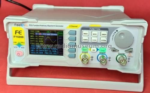
DDS Function/Arbitrary Waveform Cenerator FY6900 /20 /30 /40 /50 /60
FeelTech Technology Co., Ltd.; Zhengzhou
- Produttore / Marca
- FeelTech Technology Co., Ltd.; Zhengzhou
- Anno
- 2019
- Categoria
- Strumento da laboratorio
- Radiomuseum.org ID
- 325414


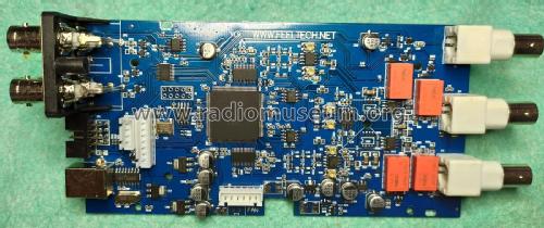
General view of the main PCB.

- Numero di transistor
- A semiconduttori.
- Semiconduttori
- Principio generale
- DSP, Processore di segnale digitale
- Gamme d'onda
- - senza
- Tensioni di funzionamento
- Alimentazione a corrente alternata (CA) / 100-240 Volt
- Altoparlante
- - - Nessuna uscita audio.
- Materiali
- Plastica (non bachelite o catalina)
- Radiomuseum.org
- Modello: DDS Function/Arbitrary Waveform Cenerator FY6900 /20 /30 /40 /50 /60 - FeelTech Technology Co., Ltd.;
- Forma
- Soprammobile con qualsiasi forma (non saputo).
- Dimensioni (LxAxP)
- 200 x 190 x 90 mm / 7.9 x 7.5 x 3.5 inch
- Annotazioni
-
The FeelElec FY6900 is being manufactured with several different chassis variants where the only difference is the Sinewave maximum frequency indicated in the model name postfix. In this unit the "-40M" indicates 40MHz, but other models are available like the 20, 30, 50 and 60MHz. The remaining parameters are identical between models.
The vast list of features can be consulted in the manufacturers website. Here is a shortlist:
- DDS direct digital synthesis technology
- 250MSa/s sampling rate, 14bits vertical resolution
- 40MHz Sine, 25MHz Square, 10MHz Ramp, Triangle, Pulse, CMOS, Arbitrary
- Dual channel output, phase adjustable, independent or synchronous operation
- Store up to 20 user defined state parameters
- 34 preset waveforms (*) and 64 user-defined waveforms (8192*14bit storage depth)
- PC arbitrary waveform editing application for remote connectivity and control
- Open remote communication protocol (USB to Serial interface, 9600bps)
- Phase adjustment between channels of 0~359.99° with a precision of 0.01°
- Linear and logarithmic scanning on frequency, amplitude, offset and duty cycle
- Burst output with optional manual, internal CH2, or external trigger
- Supports the output function of each parameter of VCO voltage control signal
- Rich modulation types: AM, FM, PM, ASK, FSK and PSK
- Accuracy ±20ppm
- Stability ±1ppm / 3hours
- Sine wave THD <0.5% (20Hz~20kHz, 0dBm)
- Square wave Rise/Fall Time ≤7ns (VPP<5V), Overshoot ≤5%
- Sawtooth wave Linearity >99% (0.01Hz~10kHz)
- Output (Vpp): ≤5MHz: 1mV~24V; 5MHz~10MHz: 1mV~20V; 10MHz~20MHz: 1mV~10V; >20MHz: 1mV~5V
- Output Resolution: 1mVpp; Flatness ±2.5% (<10MHz); ±5% (>10MHz)
- DC offset ≤20MHz: ±12V; 20MHz: ±2.5V; Resolution up to 1mV
- Output Impedance: ~ 50Ω±10%(Typical)
- Output short circuit protection for more than 60s
- TTL Output Amplitude >3Vpp; Fan-out >8 TTL load; Rise/Fall Time ≤10ns
- CMOS Output Low Level<0.3V; High Level1V~12V; Rise/Fall Time ≤18ns
- Pulse wave pulse width adjustment range of 20ns to1S
- 100MHz Meter/Counter: DC/AC, Frequency, Period (>5nS), Pos/Neg Pulse Width, & Duty Cycle
- 100MHz Meter/Counter input voltage range: 1Vpp~20Vpp
- Size: 200mm * 190mm * 90mm (L * W * H)
- Weight: 850g
(*) Sine, Square, Rectangle (Duty Cycle adjustable), Pulse (Pulse width and cycle time can be set accurately), Triangle/Ramp, Sawtooth Wave, CMOS, Four channels TTL, DC, Half wave, Full wave, Positive Step, Inverse Step, Positive Exponent, Inverse Exponent, Lorenz Pulse, Multitone, Noise, ECG, Trapezoidal Pulse, Sync Pulse, Narrow Pulse, Gauss White Noise, AM, FM, and other 64 sets customer-defined waveform
- Peso netto
- 0.850 kg / 1 lb 14 oz (1.872 lb)
- Prezzo nel primo anno
- 84.00 EUR
- Bibliografia
- - - Manufacturers Literature
- Autore
- Modello inviato da Jose Mesquita. Utilizzare "Proponi modifica" per inviare ulteriori dati.
- Altri modelli
-
In questo link sono elencati 3 modelli, di cui 3 con immagini e 0 con schemi.
Elenco delle radio e altri apparecchi della FeelTech Technology Co., Ltd.; Zhengzhou
Collezioni
Il modello DDS Function/Arbitrary Waveform Cenerator fa parte delle collezioni dei seguenti membri.
Discussioni nel forum su questo modello: FeelTech Technology: DDS Function/Arbitrary Waveform Cenerator FY6900 /20 /30 /40 /50 /60
Argomenti: 1 | Articoli: 1
This series of FY6900 signal generators were announced by FeelElec around 2019 on eevblog and this model toghether with the previous FY6600 are probably the most dissected and discussed SigGen in the forums for the good (low price, good specs, diy mods) and bad (questionable fiability, bugs and the infamous 4nS jitter) reasons.
FeelElec has announced this model as an upgrade of the FY6600 series where features like MagicPulse Technology with Low Jitter(RMS)<200ps, more than 100 Waveforms: 8192 points * 14bits, and 0~24Vpp output amplitude range,with minimum resolution of 1mV.
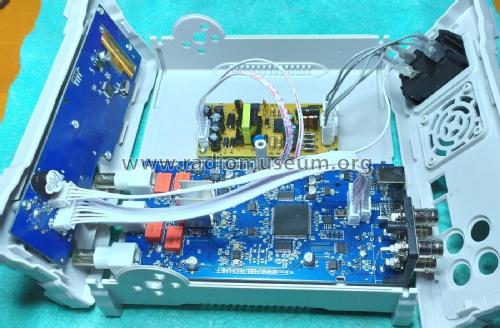
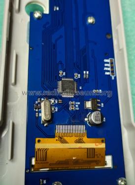
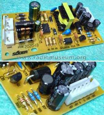
This FY6900 consists of these main assemblies: The Power Supply, the Main PCB (Signal Board), and the Front Panel PCB (MCU Board).
The Switching Power Supply may be adequate to support the requitred current consumption of the +5V and +13.5V and -13.5V, but it is probably the weakest part of the unit.
There are at least two Signal Board PCB revisions: V1.8 and V1.9, where the V1.8 still used the Altera Cyclone 4 FPGA, and V1.9 started to use a FeelElec-PRO 1941 FPGA and a Fan power supply header was included (despite no Fan is supplied up to Nov-2020).
There are also two known PCB revisions for the MCU Board, V1.8 (that goes with Signal Board V1.8), and V1.91 (That goes with Signal Board V1.9).
The known firmware releases are 1.2, 1.3 (around Nov-2019), and 1.4 (around Oct-2020). The management firmware is selfcontained inside the Front panel MCU Board MCU IC (STM32F103C8 ARM Cortex-M3 32-bit MCU 64KB Flash). Howeve the signal shaping firmware for the FPGA is contained inside a Winbond 25Q16JVS10 Flash ROM IC in the Main PCB Signal Board. FeelElec reports that firmware upgrades are done at the factory only (they can sell the two ICs (MCU and Winbond Flash) for those able to use a solder iron). That said, some customers have reported that they were able to update the firmware online by using the PC Software v6.5 (FY6900 remote control software) by installing the available PC Software V6.3 from FeelElec website, then do a online update to 6.5, and finally updating the firmware from 1.3 to 1.4 (firmware below 1.3 do not support online updates), but FeelElec has reported that this method was in beta testing and should not be used until the PC Software 6.5 is stable to be officially released on their website (this was the response from my AliExpress seller yesterday, Nov-18, 2020).
Some anomalies were reported on the forums, like:
- The electromagnetically noisy Switched Power Supply supplying the +13.5V & -13.5V used by the high voltage output Opamps for the lower frequencies. This noise is also visible on a scope set to 5mV/div by selecting zero volt from the Signal Generator: a complex pattern with 67KHz 2mVpp bursts consisting of very high RF frequency and a minor 50Hz modulation as well is visible; swithing off the Signal Generator eliminates this noise. Some of this noise is coming from the SPS, other RF high frequency are most probably coming from the LSI chips.
- This SPS is not shielded in a metal case and the output power cable is not filtered with any sort of ferrite clips or similar noise killing devices. Also the SPS PCB is installed very close to the Signal Board.
- Distorted squarewave above 5V signal output for frequenciess of 10MHz and above, a clear indication of the poor Opamps implementation used in the high voltage section of the output amplifier;
- Non normalized 86 Ohm attenuator pad for outputs below 500mV (50 Ohm should be the accepted nominal value);
- Output DC Offset is not zero Volts for all frequencies and voltages, a minor issue.
FY6900 Parts list
Front Panel PCB V1.91 (Managemnent Board)
U1 STM32F103C8 ARM Cortex-M3 32-bit MCU 64KB Flash
SU1 AMS1117 3.3 LD918 3.3V Regulator
XTAL 8B000G4CP 8MHz oscillator
LS1 Buzzer
LCD Standard ILI9341 ?
FS1 8-pin Connector to MCU
J1 4-pin Connector to MCU: RXD, TXD, GND, 5V USB to serial CH340 on the main board
JK1 4-pin header to MCU. GND, 3V3, JTCK, JMS
Note on JK1: It could be used to connect the MCU to an external programmer like the "ST-Link V2 programmer" to R/W the STM32 MCU Flash memory.
Main PCB V1.9 (Signal Board)
U2 FeelElec-PRO 1941 FPGA
U? DAC904? 165MHz overclocked to 250MHz
U? DAC904? 165MHz overclocked to 250MHz
U16 CETECJ 10.000 166 4-pin SMD 10MHz Oscillator close to FPGA
U? Winbond 25Q16JVS10 8-pin SMD Flash ROM close to U16 and FPGA
U? MCP4822E SN 2017 8-pin SMD after FPGA
U? MCP4822E SN 2017 8-pin SMD after FPGA
U? AD8009 ARZ #549 8-pin SMD low voltage Opamp after DAC904 & LBPF
U? AD8009 ARZ #549 8-pin SMD low voltage Opamp after DAC904 & LBPF
U? 4556A JRC 8-pin SMD Opamp after 2 x MCP4822E
U? 3002I 3VT 8-pin SMD high voltage output opamp
U? 3002I 3VT 8-pin SMD high voltage output opamp
U7 HC245 XR00611 20-pin dip SMD close to back panel, rear side of FPGA
U? 4558D JRC 8-pin SMD close to U7
U? CH340G 16-pin dip SMD for USB / Serial I/O
U? 12.000 12MHz Crystal
U13 AMS1117 1.2 1.2V REG SMD
U20 AMS1117 2.5 2.5V REG SMD
U14 AMS1117 3.3 3.3V REG SMD
T5 79L05 -5V REG SMD
T2 78L05 +5V REG SMD
RL1 EA2-5 NEC Relay output
RL2 EA2-5 NEC Relay output
RL3 EA2-5 NEC Relay output
RL4 EA2-5 NEC Relay output
ID1 T4 Diode close to relay
ID2 T4 Diode close to relay
ID3 T4 Diode close to relay
ID4 T4 Diode close to relay
Q9 J3Y 3-pin TR close to ID1
Q10 J3Y 3-pin TR close to ID2
Q11 J3Y 3-pin TR close to ID3
Q12 J3Y 3-pin TR close to ID4
A1 C14J 5-pin SMD close to Q8
Q8 A7 3-pin SMD close to Counter input BNC
Q5 J3Y 3-pin TR close to T2 78L05 REG
T1 A19T 3-pin TR close to Q5
Jose Mesquita, 19.Nov.20