Tube or NPN quasi-complementary Totem-Pole
Tube or NPN quasi-complementary Totem-Pole

Fellow radiophiles,
Two tubes or two NPN transistors can be configured in a push-pull power amplifier that requires no additional phase inverting stage or drive transformer. This configuration is known as Quasi-Complementary, and the stacking arrangement of the tubes or transistors recalls a native-American Totem-Pole.
There are at least two RMorg threads addressing this mode of operation. One thread focuses on an implementation with NPN transistors and the other focuses on the Tube implementation. These two threads are in German. I used Google-Translate to read them in English.
I became aware of the tube version when Henning Oelkers mentioned it in post 2 of the NPN version.
This circuit is very simple, but the analytical determination of gain and impedances is not as straight-forward as with more conventional circuits. I will attempt an analysis here. I took several approaches to the analysis in an attempt to gain a fuller understanding of the operation.
The following is my annotated version of the schematic that was posted by Christian Bruckner in the NPN Transistor thread.

All the numbers shown were taken directly from nearby component values.
Bias levels
The bias voltages are the easiest to calculate. Both input and output stages are biased by base current drop across R3, R6 and R7, for Q1, Q2 and Q3, respectively.
Q1
The calculation for Q1 involves the assumption that the base will operate around 0.68V, leaving 9-0.68=8.32V to drop across R3 and R4.
The current gain Beta=115 for Q1 forces 115 times more current into the collector than into the base. This means that the R3=470k base resistor, when shunted to the collector current, looks 115 times lower in impedance, for a net 470k/(115+1)=4.1k.
Now we have a simple voltage divider between the collector load R4 and the R3//Q1collector. Not surprisingly, this divider sets the collector voltage halfway down the 9V supply at 4.5VDC.
The standing current is simply the voltage drop from the supply to the base divided by the two calculated series impedances: (9V-0.68)/(4.1k+4.7k)=0.92mA
This current level translates directly to a transconductance gm=0.92mA/26mV=1/28R=36mS at room temperature. The thermal voltage Vt=26mV is proportional to absolute temperature in Kelvins. This Vt number is also valid for all silicon transistors.
Q2 and Q3
A very similar bias technique was used for Q2 and Q3, except that they are both in series with R8=10R.
The much lower base bias resistors R7=R6=47k combine with the higher rated Beta=200 for a shunt resistance for each transistor branch of 47k/(200+1)=235R.
The voltage drops for 235R in series with 10R and 235R calculate to 4.58 at the amplifier output, with 160mV drop at R8=10R.
The output stage standing current is calculated from the supply voltage, with the two Vbe drops subtracted, and divided by net series resistance (9V-0.65-0.65)/(235R+10R+235R)=16mA
Repeating the gm calculation for Q2 and Q3, we get Q2gm=Q3gm=16mA/26mV=1/1.6R=625mS.
Gains
The overall voltage gain from the base of Q1 to the speaker terminals at mid-band is 480, with Q1 cntributing a voltage gain of 4 and the combined action of Q2 and Q3 contributing a gain of 61.
Q1 works as a high impedance buffer with some voltage gain.
Q1 contributes a larger current gain than it does voltage gain. The input impedance of Q1 is Beta/gm=3.25k, while the impedance at the output of this stage is 120R. The impedance seen at the output of Q1 is dominated by the low impedance of 120R seen at the input of Q2 This works out to an impedance transformation of 1/27.
The current gain from the base of Q1 to the input of the output stage is approximately Q1Beta=115, because the 120R load absorbs nearly all amplified signal currents away from the collector pull-up load R4=4.7k.
Q2 drives Q3 through R10
As prof. Rudolph points out in Post 7 of the thread about the implementation with NPN transistors, the coupling from Q2 to Q3 is done via R8=10R.
Q2 is a conventional common emitter stage, just like Q1, with an output impedance that is 47k*Q2Beta=235R.
This impedance drives the Q3 stage in parallel with the speaker load via R8=10R.
Speaker impedance
The speaker load is unknown, but we can reasonable estimate a reasonable range of loads from C6=125uF, if we assume that the low frequency corner of the audio band for this lower power amplifier is 100Hz. This would gives the lowest acceptable impedance for the speaker as 12R.
I chose an arbitrary 100R speaker load impedance. This would give improved bass response with headphones. This also gives the highest average power output. The highest average power output is a function of the highest average available current under the highest available voltage swing. This is not the same as matching of impedances between speaker and amplifier.
Another reasonable approach to bound the range of reasonable speaker impedances, is to match the speaker impedance to closed loop amplifer output impedance. I calculated the output impedance of the amplifier as 20R, so a 20R speaker would deliver the highest power gain, but at a lower maximum power than the 100R load. The 20R load would be preferred to drive an earphone, where the highest gain might be desired.
This amplifier was able to deliver in an LTspice simulation up to 4Vp-p with a 100R load. This is plenty for headphones, or just enough for a small speaker.
R8=10R operation
The output stage depends critically on R8=10R for it's operation. R8=10R couples signal from Q2 Collector to Q3 base via C5 and R9. R10 also samples the speaker load current to drive the base of Q3.
During the DC bias point analysis I ignored R9=1k because it was in series with C5=10uF. The AC analysis requires that C5 be approximated with a short.
The impedance of the upper half of the output stage surrounding Q3 is much higher at AC because of the sampling of signal via R8=10R and coupling to the base of Q3 via R1. The net impedance of the upper half calculates to 2.4k, if the speaker impedance is not included. This is a very high load impedance for the 235R output impedance of the lower half of the output stage Q2.
But when the Speaker load is AC coupled to the emitter of Q3, the load impedance posed by Q3 rises because of the current sampling by R8=10R boostrapping the base of Q3 via R0=1K. The net load impedance for Q2 becomes is almost exclusively dominated by the very low Speaker impedance.
Prof Rudolph also points out the inversions in the signal path. There is a signal inversion from the Q2Base to Q2Collector. When Q2 pulls more current from the speaker load, the drop across R8=10 reduces current in Q3. So we have another inversion from the Q2Collector to Q3.
If there is no speaker load, the current through Q3 increases when the current through Q2 increases and there is no longer an inversion from Q2 collector to Q3.
This shows that the operation of Q2 and Q3 is complementary only in the presence of a speaker load. This explains why "Quasi" qualifies the complementary operation of Q2 and Q3.
Without a speaker load, the upper half of the output stage comprising Q3, R8, R9 and R6 are AC-equivalent to a 2.4k resistor.
Node Voltage Derivation of Q3 stage
See NPN_Totem_Pole_analysis for a formal derivation of the behaviour of stage Q3. One interesting result from this formal analysis of the Q3 stage is that it roughly doubles the impedance of the speaker, as seen by the Q2 stage. This makes perfect sense, if Q2 and Q3 are going to share the load equally. Someone did a pretty good job designing this amplifier.
Negative Feedback
R10=22k in parallel with R7=47k apply negative feedback around two stages of gain Q2 and Q3. One effect of this negative feedback is to lower the load impedance for the first stage Q1 to 120R. In this case, the drop across R8=10 can be negleted, so that R7=47k is approximately in parallel with R10=22k.
Negative feedback is a primary factor setting the voltage gain of the first stage Q1 by setting it's load impedance.
Simulation
I used approximate transistors in the following LTspice simulation. I tweaked the value for Beta to match the specified value of the original schematic. You can contact me for the LTspice simulation files at my email "k2w at PhilbrickArchive dot org". LTspice is a free simulator from www.linear.com.

The simulated results are in fair agreement with the calculated operation.
Class A
So far I have made every approximation in my analysis with a linearized element, but the full power swing of this amplifier with a 100R speaker load delivers 25mW with a 4Vp-p swing at the speaker and distortion at the 2nd Harmonic is -30dB.
The tube example
The Tube implementation mentioned at the top of this post is for a Philips BX2553A. This radio is one of the very few that have not transformers of any kind in it's audio stages. The Quasi-Complementary Totem-Pole topology needs no input inverting driver stage, and the 800R Speaker load also eliminates the need for an output transformer.
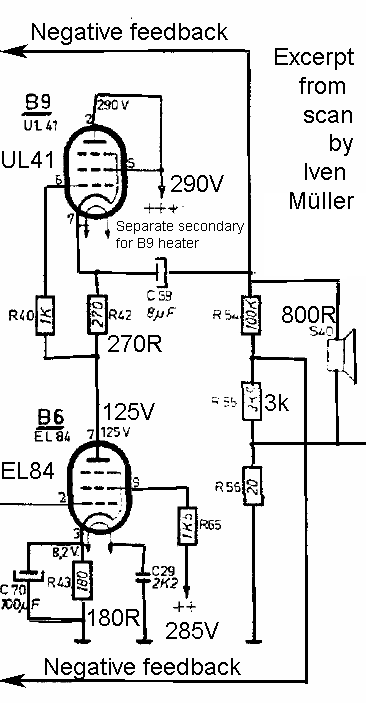
Very much like with the NPN example above, capacitor coupling is used throughout.
With a manufacturing date of 1955, it is most likely that this topology existed with tubes before it was implemented with transistors.
This stage has a topology that is very similar to the NPN topology, The same analysis can be applied here.
R42=270R corresponds to R8=10R above.
There are no pull-up Grid resistors to correspond to the pull-up Base resistors. Beta can be thought to be infinite in the tube case.
The transconductance for the UL41 is specified as 9.5mS and it is 11mS for the EL84.
The Grid bias is simpler than base bias. R40=1k just prevents parasitic oscillation trouble. The Grid of the UL41 is driven directly by the plate of the EL84 at audio frequencies.
Another note-worthy difference is that the UL41 is essentially triode connected with a typical voltage drop of 165V, while the EL84 still functions as a pentode with a 285V screen bias. The Pentode operation of the EL84 allows for plate voltage as low as 50V. The UL41 has no requirement for plate operation below the screen.
These differences in the operation requirements between the two tubes explain the different choice of tube types.
Hans Knoll explored the operation of this stage in Post 4 of the Tube implementation
Note that the UL41 heater has a separate transformer winding that is connected to it's cathode. If the same grounded heater power source that is used for the other tubes, were used for the UL41, the heater-cathode voltage rating would be exceeded.
Node Voltage derivation of UL41 stage
See Tube_Totem_Pole_analysis for a formal derivation of the operation of the UL41 stage. The derivation of the UL41 stage is even simpler than the derivation for the equivalent Q3 stage above. As was found with the NPN example, the UL41 stage presents a net load impedance of 1410R to the EL84 that is nearly double the 800R speaker impedance. Again, this is very good load sharing between the dissimilar UL41, and EL84 tubes.
Another Push-Pull topology without phase inverters

In the tube era there were push-pull stages that did not have a separate phase-splitter driver or phase splitting transformer.
The Philco 40-185 has no phase splitting tube, or phase splitting transformer, to drive the 41 tubes in push-pull.
The upper output 41 tube takes it's drive from the audio preamp, and supplies an inverted signal at it's screen grid that is attenuated against it's input signal to drive the control grid of the lower 41 with a net gain of -1.
The negative feedback supplied by (48) helps to make the net gain from the upper 41 control grid to the lower 41 control grid equal to -1, despite variations and mismatch in tube gain.
Class A Push-pull operation results at the plates with a center tapped transformer load. Class AB is not possible because the upper tube must always be active to drive lower tube.
The coloured arrows mark the audio signal polarity and flow through the output stage.
This output stage can still be considered fully complementary because it does not depend on the speaker load for signal, as is the case with the Quasi-Complementary Totem-Pole topology.
Comments or corrections invited,
Regards,
-Joe
Two notation errors were corrected with the kind notice from Marc Gianella. One error was in the notation for the bias resistors for Q1 in the bias level discussion. The other error was a reversal of the calculation for the input impedance of Q1 in the gains discussion.
Thanks, Marc.
-Joe
To thank the Author because you find the post helpful or well done.