|
2
a extract from the patent application of the Tektronix tube
United States Patent [19] [11] 3,748,585
Culter et al. [45] July 24,1973
[54]
SILICON DIODE ARRAY SCAN CONVERTER STORAGE TUBE AND METHOD OF OPERATION
[75] Inventors: Robert Gordon Culter, Portland;
Raymond Hayes, Beaverton;
Emmanuel Sang, Portland, all of Oreg.
[73] Assignee: Tektronix, Inc., Beaverton, Oreg.
[22] Filed: Nov. 15, 1971
[21] Appl. No.: 198,582
[56] References Cited
UNITED STATES PATENTS
2,713,648 7/1955 Gardner 328/124 X
3,356,878 12/1967 Yaggy et al 315/12 X
3,360,680 12/1967 Plaistowe 315/12 X
3,440,476 4/1969 Crowell et al 313/66 X
3,675,134 7/1972 Leudicke et al 328/124
3,676,727 7/1972 Dalton et al 313/66
Primary Examiner John S. Heyman
Attorney Adrian J. LaRue
ABSTRACT
A silicon diode array scan converter storage tube is disclosed which, after a diode array target has been electrically prepared, has information written an the diode array target in a writing mode, the information is transferred to an müde coating of the target to store same, and the target is subjected to a scanning mode while being illuminated, thereby producing an electrical readout signal corresponding to the stored information thereon.
12 Claims, 6 Drawing. Figures
SILICON DIODE ARRAY SCAN CONVERTER
STORAGE TUBE AND METHOD OF OPERATION
BACKGROUND OF THE INVENTION
Diode array targets have been used in vidicon tubes wherein optical images are applied to one side of the diode array target which produce charge images and the other side of the target is continuously scanned by an electron beam to read out the charge pattern images therefrom.
In another application, a charge pattern image formed by an optical image on the diode array target is transferred to the oxide surface surrounding the photodiode so that the image is stored thereon and the stored image can be read out via the electron reading beam for several minutes or stored for longer periods of time.
The scan converter storage tube of the present invention is useful to write information on a silicon diode array target by means of an electron beam instead of using an optical means.
The scan converter storage tube of the present invention is especially useful to prepare the silicon diode array target at a different time from transferring the written information onto the oxide coating of the target which is separated by the writing Signal.
The scan converter storage tube of the present invention has the ability to store written or defect areas which are either bright or dark and cancels defects by combining modes of dark and bright storage.
Targets, which have a high average dark current and which have storage times unsuitable for normal scan conversion operation, can still be used in accordance with the principles of the present invention; these targets may not require illumination during the read mode of operation.
An object of the present invention is therefore to provide a scan converter storage tube having a storage target which includes a first means that is electronically charged when a writing electron beam is deflected there along in accordance with an input signal to produce a charge pattern thereon and a second means for storing the charge pattern thereon.
Another object of the invention is the provision of a scan converter storage tube wherein the storage target is prepared at a different time from transferring the information onto the second means of the target which is separated by the writing signal.
A further object of the invention is to provide a scan converter storage tube in which the prepare mode of operation is for an indefinite period of time and the transfer mode of operation, whereby the Information written on the first means of the storage target is transferred to the second means is triggered by the writing mode of operation.
A still further object of the invention is the provision of storing defects and written information on a storage means of a scan converter storage tube and cancelling the defects prior to reading out the written information.
Still another object of the invention is to provide a method of preparing, writing, transferring, storing and reading information of a scan converter storage tube.
BRIEF DESCRIPTION OF THE DRAWINGS
Other objects and advantages of the present invention will be apparent from the following detailed description of certain preferred embodiments thereof, and from the attached drawings of which:
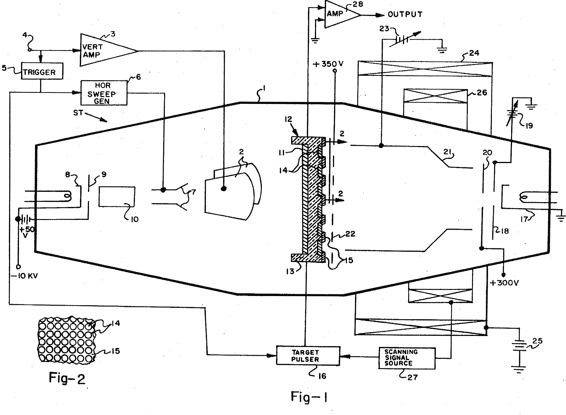
FIG. 1
is a schematic diagram of one embodiment of the storage apparatus of the present invention;
FIG. 2
is a view taken along line 2-2 of FIG. 1 showing the reading surface of the storage target on an enlarged scale;
FIG. 3
illustrates waveform diagrams showing the Operation of the first embodiment;
FIG. 4
illustrates another waveform illustrating the operation of another embodiment;
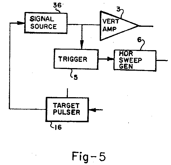
FIG. 5
is a part schematic diagram of a further embodiment;
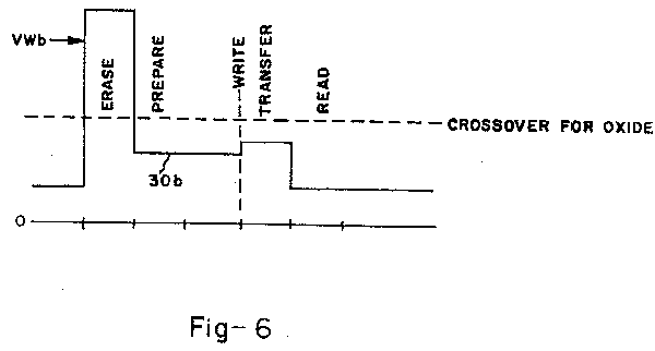
FIG. 6
illustrates the waveform diagrams showing the operation of the further embodiment.
DESCRIPTION OF THE PREFERRED
EMBODIMENTS
A scan converter storage tube ST illustrated in FIG. 1 is provided with an evacuated envelope 1 which is
preferably glass, but it can be made from any suitable dielectric material. The electrical signals to be displayed are applied across a pair of vertical deflection plates 2 of an electron gun, at least one of which is connected to a vertical amplifier 3 which in turn receives input signals from input terminal 4. A trigger circuit 5 is connected to the input from terminal 4 and its output is connected to horizontal sweep generator 6 which is connected to at least one of horizontal deflection plates 7.
A cathode 8 is located at one end of the tube and it is connected to a minus 10 kv. voltage for generating a high velocity beam of electrons through a control grid 9, which is connected to a minus 50 volt supply, a focusing anode or lens structure 10. The horizontal sweep generator 6 applies a conventional sawtooth or ramp-shaped sweep signal across horizontal deflection plates 7 when trigger 5 is actuated by input signals applied to input terminal 4 thereby triggering horizontal sweep generator 6 and the input signals are also amplified by vertical amplifier 3 and then applied to vertical deflection plates 2 thereby causing the electron beam to be deflected along a writing area 11 of a diode array storage target 12, which is similar in construction to that disclosed in U.S. Pat. No. 3,440,476. Information may also be written onto writing area 11 of storage target 12 by optical means in accordance with conventional techniques. Writing area 11 constitutes a thin region of N-type material such as, for example, phosphorus-doped silicon to provide an N plus layer within an etched area of an N-type silicon wafer 13 which has P-type regions 14 formed within wafer 13 to form a planar array of P-N junction diodes thereby providing a plurality of discrete P-N junctions with respect to common substrate 13. An insulating coating 15 of silicon dioxide, silicon nitride, or the like, covers the reading area of target 12 and overlaps the exposed edges of the junctions.
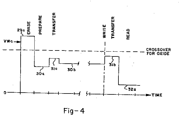
A target pulser circuit 16 of conventional design is connected to target 12 to provide operating voltages in accordance with the voltage waveform VW of FIG. 3 thereto and it is connected to trigger circuit 5 to cause pulser 16 to operate in synchronism with the input signal. Voltage waveforms VWa of FIG. 4 and VWb of FIG. 6 are also produced by pulser 16.
The target pulser 16 contains an electronic switching circuit which connects the target lead to various voltage levels. The switches are controlled by gates which are connected to timing circuits and to inputs from the scanner 27 and trigger 5 to produce the voltage waveforms shown in FIGS. 3, 4 and 6.
The reading beam assembly is substantially conventional and includes an electron gun 17 connected to ground, a control grid 18 connected to a negative voltage 19 which is variable between -70 v. and ground, an accelerating grid 20 connected to +300 v., a focus barrel 21 and a deceleration grid 22. The focus barrel 21 is connected to a variable voltage 23 which has a maximum voltage of 300 v. Grid 22 is connected to a +350 v. supply.
The reading electron gun assembly is surrounded by a magnetic deflection assembly comprising a focus coil 24, which is connected to a DC supply 25, and a deflection coil 26, which is connected to a scanning signal source 27. The reading electron beam can thus be scanned over the reading area of target 12 by this magnetic deflection assembly. Scanning signal source 27 is connected to target pulser circuit 16 and causes same to operate thereby assuring that target voltages changes occur during the scan flyback Operation.
Target 12 is connected to one input terminal of an amplifier 28 while the other input of this amplifier is connected to ground. The output from amplifier 28 is a video output which is connected to a television monitor to display the information that is being read out from target 12.
The operation of the embodiment of FIG. 1 will now be discussed with reference to FIG. 3. Target pulser 16 is actuated in accordance with the operation of scanning signal source 27 to provide waveform VW of FIG. 3 which provides voltage levels at time intervals representative of target scanning intervals. The oxide charge differences of substrate 13 and oxide coating 15 defining oxide areas of target 12 are erased by voltage waveform VW being raised to level 29 above the crossover level for the oxide thereby allowing all the oxide areas to charge to the same level. Target 21 is then brought to voltage level 30 below the oxide crossover level so that the oxide areas are charged down to near the scanning gun cathode potential.
Target 12 is then scanned by the scanning beam at voltage level 30 to establish a charge across all diodes 14 thereby defining a prepare level which can be depleted by the writing beam when it is caused to be impinged thereon. This prepare scanning operation at voltage level 30 continues for an indefinite period of time until an input signal occurs at input terminal 4 whereupon the signal is amplified by vertical amplifier 3 and applied to vertical deflection plates 2 and causes trigger 5 to trigger horizontal sweep generator 6 which controls horizontal deflection plates 7 thereby controlling the writing beam to write the input signal on the writing area of target 12 and the output from trigger 5 also triggers target pulser 16 which causes certain areas of target 12 to be written producing more positive diode surfaces.
After the information has been written onto the writing area of target 12, the target is raised to voltage level 31 at the beginning of the next scanning frame causing the information to be transferred to areas of oxide coating 15 corresponding to the written areas of target 12. During the transfer operation, more charge will be drawn to the written diodes than the unwritten ones. As a result, the oxide areas adjacent to the unwritten diodes will be charged closer to ground.
The voltage is lowered to level 32 defining the read Operation and illuminated strongly as represented by voltage level 33 of waveform 34; voltage level 35 representing that the target illumination is in an off condition. The target 12 can be illuminated by use of light emitting diodes or incandescent light means inside or outside of tube envelope, scanning writing beam over entire target or scattering electrons from writing beam.
The oxide coating adjacent unwritten areas of the target will be switched to a level low enough to cut off the reading beam resulting in a dark background. Oxide coating adjacent written areas cannot cut off the beam and these areas appear bright. Illumination is necessary so that diodes act as collector areas. Very leaky targets require little or no illumination.
Alternatively, dark stored information on a bright background can be obtained using a higher or lower transfer voltage level 31 than that described hereinabove:
The electrical readout signal produced during the reading operation of target 12 is supplied to amplifier 28 and the output therefrom is transmitted to the Z-axis input at the control grid or cathode of a remote TV monitor tube (not shown) to display the information.
The foregoing description is in conjunction with the occurrence of some event such as, for example, high Speed transient signal which will occur at some unspecified time and a diode array target having no faulty diodes which are very leaky.
Since faultless diode array targets are extremely difficult to make, leaky diodes are present in most diode array targets which provide faulty diodes that create bright spots thereby providing improper information in some or many cases.
In order to eliminate or substantially minimize such bright spots created by the leaky diodes, voltage waveform VWa of FIG. 4 is generated by target pulser circuit 16 in FIG. 1 and it is essentially the same as waveform VW in FIG. 3 except that after the voltage level has been lowered to voltage level 30a from level 29a, the voltage level is raised after a time interval to voltage level 31a constituting a first transfer operation whereby the leaky diode areas are transferred as dark areas onto the oxide coating 15 along with any other areas that may be providing faulty information. Thereafter, the voltage level is changed to a second prepare voltage level 30b.
After the write cycle of operation, the voltage level is raised to level 31b which is higher than level 31a and which is a second transfer operation to transfer the information and leaky diodes as bright areas onto oxide coating 15 and this will cancel or minimize the stationary special noise of die leaky or faulty areas of target 12 when the voltage level is lowered to level 32a defining the reading operation of target 12.
An alternative voltage waveform can be used to operate target 12 whereby the first transfer voltage level 31a can be higher than second transfer voltage level 31b which will cause the faulty target areas to be transferred as bright and dark areas respectively onto the oxide coating.
A further voltage waveform can be used to operate target 12 whereby both transfer voltage levels can occur after the writing operation as first dark and bright or vice versa as desired. Thus, even though a diode array target has faulty or 5 leaky diode areas, such target can still be effectively used when using the waveforms as described hereinabove to operate target 12.
FIG. 5 illustrates another embodiment of the present invention wherein input signal source 36 is controlled by target pulser 16 so that the writing Operation by the writing gun can occur as soon as the prepare operation has been completed by the voltage level of voltage waveform VWb being lowered to voltage level 30b; otherwise, the tube is operated as hereinbefore described.
While there has been shown and described various embodiments of the present invention, it will be apparent to those skilled in the art that many changes and modifications may be made without departing from the invention in its broader aspects. The appended claims are intended to cover all such changes and modifications as fall within the true spirit and scope of this invention.
….
Attachments
|