grundig: Circuitry Analysis 5040W/3D - Part 5
grundig: Circuitry Analysis 5040W/3D - Part 5

This thread is a translation of a German language thread schaltungsanalyse_5040w3d_5_teil, which is 5th in a series of discussions of the circuitry design of the Grundig 5040W/3D. English translations of the previous four threads are here:
- Tom A.
(Translation of text originally by Thomas Günzel)

Dear friends of the forum,
First, let me thank everyone who has participated in these circuitry analysis discussions so far. Many people have undoubtedly said "Aha!" a few times when they have understood something for the first time by reading the explanations here.
Before we could proceed with discussions of the AM section, I had to make some significant revisions to our working schematic diagram. The versions I was working with had a lot of errors in some parts.
Therefore, from now on, please use Version 1.4 of the Schematic as the basis for further discussion!
Nonetheless it isn't so simple to recognize all the relationships between different parts of the circuitry. Therefore I have extracted various parts of the circuitry to visually simplify the analysis.
Here is the first question:
The input selection for the short wave bands is presented as follows:
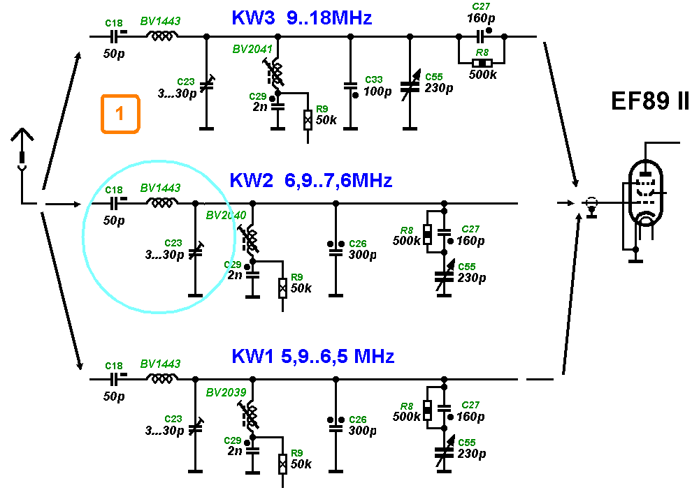
What is the purpose of the combination of C18, BV1443, and C23, which is the same for all short wave bands and therefore must cover the range of 6-18 MHz?
Enjoy,
Thomas G.
To thank the Author because you find the post helpful or well done.
Answer to Question 1
(Translation of text originally by Thomas Günzel)
Dear friends of the forum,
I received the following e-mail from Herr Bernhard Nagel:
I've been following with great interest the previous discussion in Part 4 of the circuitry analysis of the 5040W/3D and I have learned a few things from it, or at least improved my understanding.
Here is a first attempt to answer question 1 in part 5.
First, there is no bandpass filter at the input for the 3 short wave bands as there is for the medium wave and long wave bands on the 5040W/3D; there is just this simple input circuit for each. C23 is the alignment trimmer for all three short wave bands. The inductance for the input circuit is BV2041, which is intended only for alignment of the KW3 shortwave band at the top end of its range. Short wave bands KW2 and KW1 provide bandspread for the 41m and 49m bands respectively. For these it is sufficient to peak the intput circuit BV2039/40 at the middle of the band, after alignment of KW3 is completed.
C18 and BV1443 (which is really a choke) form a bandpass filter, which works as a very simple preselector. It serves to block frequencies which are far below and far above the band of interest, especially to block FM signals from reaching the RF and mixer stages when operating on short wave. FM stations could otherwise end up mixing with harmonics of the short wave oscillator and cause interference. The Q of coil BV1443 should be low, so that the circuit can have broad bandwidth.
What I'm still wondering about: For the 3 short wave bands, an image rejection of 70-75 dB is claimed, which in my opinion should not really be possible with this kind of preselector. (Source: Grundig service information for the 5040W/3D, title page)
Regards,
Bernhard Nagel
Thanks a lot for your contribution,
Thomas G.
To thank the Author because you find the post helpful or well done.
Image rejection?
(Translation of text by Hans M. Knoll)

Hello Herr Nagel, Hello Thomas,
Since the explanation is perfect, I can stop here.
Everything was answered properly, even the part about reception of FM signals!!
Herr Nagel also saw, that even though Thomas G. had to show C23 in 3 places, it is only adjusted at 17.5 MHz. If he got that from the service manual, that's fine -- we don't make use of that often enough.
The image rejection specifications from Grundig can't be correct.
If we can temporarily agree on a spec of 20 - 26 dB (between 1:10 and 1:20 attenuation), that may be reasonable. The spec in the document is totally impossible.
Good job on noticing that!
Regards, Hans M. Knoll
Just an update - to be deleted later:
Today I have the choke, and tomorrow I'll have the inductance value and the self-resonance frequency.
This was Grundig's best short wave choke. Lots of inductance and very little self-capacitance.
The same was true of many types -- also in this model at the antenna input, to allow the FM antenna to serve as a AM antenna.
At GRUNDIG a value of 50 pF was always assumed for a "short" antenna and a value of 200 pF in series with a 400 ohm resistor for a "normal" antenna.
A typical FM whip antenna has 33 to 45 pF, depending on whether it is upright or inclined.
Addendum: I just worked a night shift.
The inductance, measured with a LARU from Rohde and Schwarz, is 4.5 uH. The resonant frequency is 22.5 MHz when connected directly between the signal generator and a diode voltmeter HP 410C with test head.
An opportunity for both of those who posted above to think over their contributions.
Best regards,
Knoll
To thank the Author because you find the post helpful or well done.
(Translation of text originally by Dieter Barkawitz)

I'm also in agreement with the explanation by Herr Nagel, but...
I would like to add that adding preselection couldn't have been the real reason that the development engineers had for making a series resonant circuit from "C18 and BV1443," since the additional amount of preselection would be pretty modest given that it is coupled to a very high impedance parallel circuit. In that case, a few hundred ohms more or less in the path from the antenna would not play a decisive role. In this case, capacitive decoupling of the subsequent parallel resonant circuit may be more important, since it is not possible to anticipate what kind of antenna the customer might attach to the receiver.
Since the antenna can be anything from a short piece of wire to a real long wire antenna, it serves as an additional unknown capacitance which detunes the input circuit in a downward direction. For this reason, in the simplest case an additional coupling capacitor is added between the antenna terminal and the input circuit. Since this coupling capacitor is permanently installed, the maximum amount of detuning due to the antenna is set. The coupling capacitor, however, has two fulfil two opposing requirements; on the one hand it should have the lowest possible impedance for the antenna signal, and on the other hand it should limit as much as possible the amount of capacitive loading from the antenna to minimize the detuning of the input circuit. The series resonant circuit fulfills these opposing requirements very well, since it has low impedance at resonance for the signal passing through, and at resonance it has no reactive component to detune the input circuit.
Unfortunately, one cannot define for the series resonant circuit a single precise frequency, which lies inside the bands that can be received; nonetheless, coupling via a series circuit still makes excellent decoupling between the antenna and the input circuit possible, since the choke also compensates a bit within the usuable frequency band.
Regards,
Dieter
To thank the Author because you find the post helpful or well done.
Image rejection redux
(Translation of text originally by Thomas Günzel)
Just now I got the following mail from Herr Nagel:
Hello Herr Knoll,
More on the subject of image rejection:
In the service manual for the 4040W/3D things are shown correctly. For the short wave bands an image rejection of 20-26 dB is specified, just as you conjectured (and consistent with experience).
In the 4040W/3D there is no choke at this point in the circuitry; there is only a capacitor (20 pF in this case) in front of the input circuit.
The coil BV1443 that we've been talking about is located on the antenna selector board, connected to one of the dipole antenna terminals.
I'm curious about the measurement result for the choke.
Regards,
Bernhard Nagel
To thank the Author because you find the post helpful or well done.
Question 2 and 3
(Translation of text originally by Thomas Günzel)
First, a "thank you" to Hans, Herr Nagel, and Herr Barkawitz for their contributions.
Here are the the next questions:
Question 2:
The input circuits for medium and long wave are tunable. How much bandwidth do these filters have, and how are they coupled?
Question 3:
From the schematic diagram, as far as I can tell, the ferrite loopstick antenna is only operational for the MW1 and MW2 bands. Is that correct, or did I overlook something?
Regards,
Thomas G.
To thank the Author because you find the post helpful or well done.
Input circuit as band filter
(Translation of text originally by Thomas Günzel)
Unfortunately Herr Bradtmöller had some problems with directly posting an answer. Here is his answer:
Hello Herr Knoll,
... The Grunding 5040, in my opinion, really only has one tuned input circuit for short wave. In contrast, for medium wave there are two. However, the whole thing has been referred to as an input band filter circuit.
Medium wave and long wave: 1-1-P-0-M
Short wave: 1-P-0-M
Example 1: (11P0M) means means two resonant circuits or bandpass filters before the RF stage, with aperiodic coupling to the mixer stage.
Abbreviations: 1 = resonant circuit, P = preamplifier, M = mixer, F = amplifier only for the ferrite antenna, 0 = aperiodic (nonresonant or untuned).
Source: http://www.oldradioworld.de/rfpre.htm (link has both English and German information in detail about RF and mixer stages of various configurations using the above terminology)
The circuit diagram at that site is different with respect to the tube placement; in principle, however, the function of the stage is as follows:
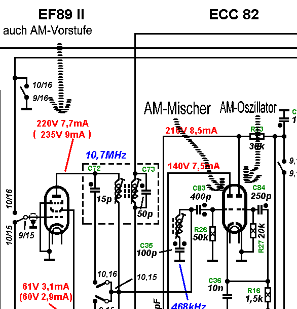
Translation for above diagram: "auch AM-Vorstufe" = also serves as AM RF stage; "AM Mischer" = AM mixer; "AM Oszillator" = AM oscillator.
Am I seeing that correctly?
With regard to answering the questions in the circuitry analysis thread, that's as far as I can go.
Just a few of my thoughts:
The bandwidth of the AM section is essentially set by the IF amplifier (9 kHz).
Since the input circuits are tunable, according to Adam Riese, the Q can't be extremely high, because a pronounced resonance at a single frequency is not desirable here. Strictly speaking, a resonant circuit, consisting of an inductance and a capacitance, has just one resonant frequency. If this is made variable, either with a variable inductance or variable capacitor, the Q, and therefore the bandwidth, varies with frequency.
Therefore, the input circuit has to have a wider bandwidth than the IF transfer curve. During alignment, the goal is uniform response, or good tracking, rather than peaking the resonance of the input circuit.
Do I have it wrong?
Using this approach, I can't give an exact answer to the question about the bandwidth of the input filter, if that's what we want to call it.
Best regards,
K.-H. B.
To thank the Author because you find the post helpful or well done.