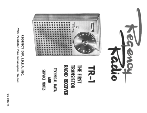
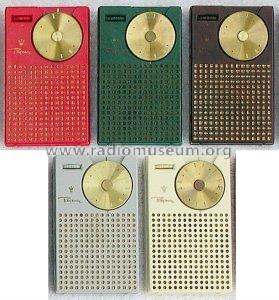
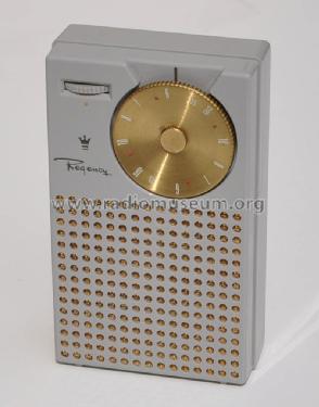
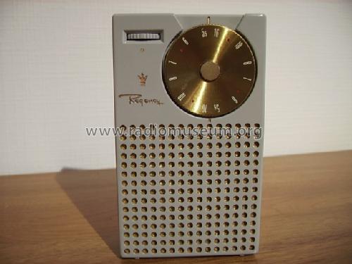
Regency TR-1 Pocket Radio
Regency (brand of I.D.E.A.)
- País
- Estados Unidos
- Fabricante / Marca
- Regency (brand of I.D.E.A.)
- Año
- 1954

- Categoría
- Radio - o Sintonizador pasado WW2
- Radiomuseum.org ID
- 71606
-
- alternative name: Idea (I.D.E.A.)


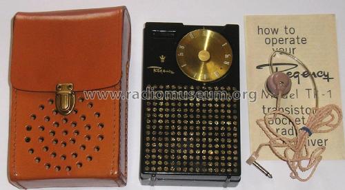
Zubehör: Ledertasche und Ohrhoerer

Ebay seller: ven-tronics, Item: 201748929951

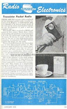
From Electronics, MAR1955.


Ebay User artinall Item 190654977620
Haga clic en la miniatura esquemática para solicitarlo como documento gratuito.
- Numero de transistores
- 4
- Principio principal
- Superheterodino en general; ZF/IF 262 kHz; 1 Etapas de AF
- Número de circuitos sintonía
- 5 Circuíto(s) AM
- Gama de ondas
- OM (onda media) solamente
- Tensión de funcionamiento
- Pilas / 22,5 Volt
- Altavoz
- Altavoz dinámico (de imán permanente) / Ø 6.9 cm = 2.7 inch
- Potencia de salida
- 0.1 W (unknown quality)
- Material
- Plástico moderno (Nunca bakelita o catalina)
- de Radiomuseum.org
- Modelo: Regency TR-1 Pocket Radio - Regency brand of I.D.E.A.
- Forma
- Portátil de bolsillo , menor de 20cm.
- Ancho, altura, profundidad
- 3 x 5 x 1.25 inch / 76 x 127 x 32 mm
- Anotaciones
-
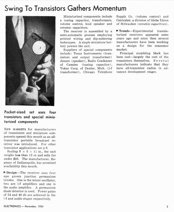
Worlds first pocket Transistor radio on the market (1954). This was organised by Texas Instruments (TI) because they looked for a popular solution for their first transistors. TI had a licence from Bell like 25 other companies to produce the then very new germanium transistor. Regency (actually then named I.D.E.A.) made transistor radios until 1960 (TR-99).
TR1 from Regency was followed in the USA by the much bigger sized Raytheon model 8TP in 4 colors but then also from General Electric model 675 in black, model 676 in ivory, model 677 in red and model 678 in green in pocket size. Sony Japan built the TR-55 for sales in August 1955.Siehe diesen Beitrag "Transistoren - der Weg dazu - frühe Forschungen - andere Möglichkeiten - erste Anwendungen" und evtl. das hier. Nachfolger des Telefunken Partner mit Röhren von 1954 ist 1956 das erste deutsche Transistorradio in Seriebau als Telefunken Partner als Vorserie TR1.
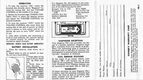
Battery ( 22 1/2V) : Regency 215
or
Burgess U 15 RCA VS084
Everready 412 Ray-O-Vac 516
General 612 Sears 8212
Zenith 212 Mallory RM 4124
Olin 1915 Sonotone 312
First sold on : Oct. 18, 1954
Date of patent application : Mar. 25, 1955
Date patented : Jun. 30, 1959
US patent : 2,892,931
- Peso neto
- 0.3 kg / 0 lb 10.6 oz (0.661 lb)
- Precio durante el primer año
- 49.95 $
- Mencionado en
- Silicon Chip magazine, April 2013, Page 84 to 88.
- Documentación / Esquemas (1)
- Radioschau Österr. 1/55
- Documentación / Esquemas (2)
- Photofact TSM Transistor Radio Series SAMS (TSM-2 (November, 1958))
- Autor
- Modelo creado por Ernst Erb. Ver en "Modificar Ficha" los participantes posteriores.
- Otros modelos
-
Donde encontrará 68 modelos, 60 con imágenes y 32 con esquemas.
Ir al listado general de Regency (brand of I.D.E.A.)
Colecciones
El modelo Regency TR-1 es parte de las colecciones de los siguientes miembros.
Museos
El modelo Regency TR-1 se puede ver en los siguientes museos.
Contribuciones en el Foro acerca de este modelo: Regency brand of I.D: Regency TR-1 Pocket Radio
Hilos: 5 | Mensajes: 7
The Regency Radio Receiver TR1 is described in "Kiver, M. S.: Transistors in Radio, Television, and Electronics, McGraw-Hill, 2nd. ed., 1959"
THE REGENCY RADIO RECEIVER
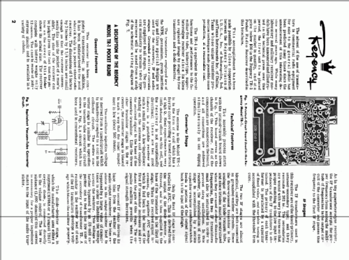
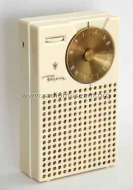
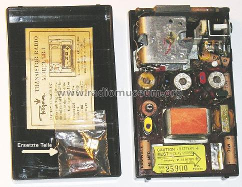
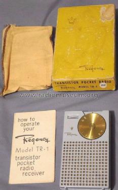
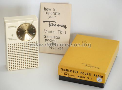
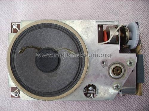
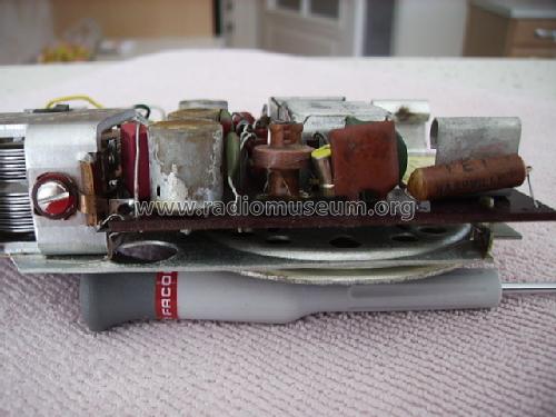
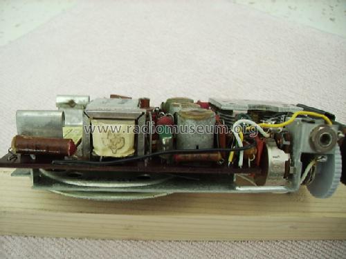
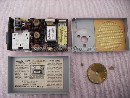
The first transistorized portable radio receiver to appear commercially was the Regency model TR 1, and it took advantage of every space saving feature afforded the transistors and associated miniature components (see Figs. 1 and 2). Over all dimensions of the unit are 5 by 3 by 1,25 in., enabling the entire set to fit easily into the pocket of a man's jacket. Weight of the set, with the batteries, is only 12 oz.

Fig.1. The Regency model TR-1 transistor radio is small enough to fit in the pocket of a man's jacket (Coutesy Regency.)

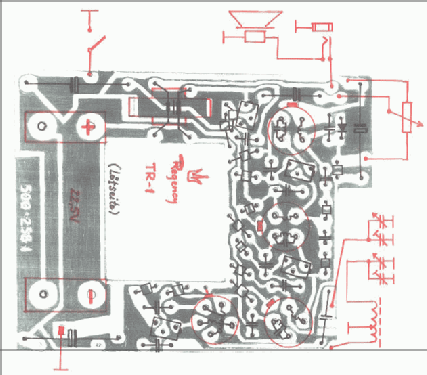
Fig.2. Inside view of Regency model TR-1 transistor receiver showing layout of components. (Courtesy Regency.)
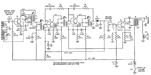
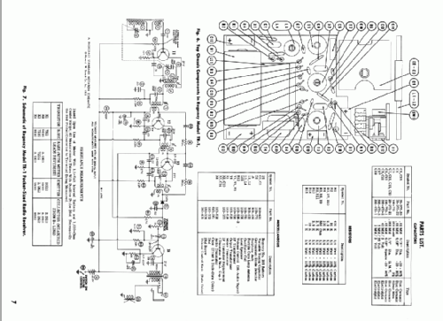
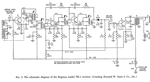
The schematic diagram of this receiver is shown in Fig. 3. There are four transistors and five stages. The extra stage is the second detector, and its function is performed by a germanium diode, here either a Raytheon CK706A or a Tungsol TS117. The transistors are of the NPN variety, and three special designs are used for the converter, i f, and audio stages. Manufacturer of these units is Texas Instruments, Incorporated.

The first stage, containing transistor V1, is essentially a self oscillating converter. The input signal is picked up by a tuned ferrite core coil which possesses a high Q. A low impedance winding on the antenna coil couples the signal to the base of V1.
Local oscillations are generated by a parallel resonant circuit in the emitter circuit which is inductively coupled to a coil in the collector circuit. The low impedance emitter is tapped down on the tuned circuit in order to provide the proper impedance match without lowering the Q of the circuit.
The foregoing oscillator arrangement is a fairly common one. Its equivalent vacuum tube circuit is shown in Fig. 4. With the incoming signal and the local oscillator voltage both being applied to the converter transistor, the appropriate i f signal is formed and then fed to transformer T1 and the i f stages beyond.

A 10,000 ohm resistor is placed in the emitter circuit to provide d c stabilization against temperature changes and variations among different replacement transistors. The positive voltage which the emitter current develops across R2 is counterbalanced by a positive voltage fed to the base from the battery. The actual voltage difference between these two elements is on the order of approximately only 0.1 volt.
The proper biasing voltage for the collector of V1 is obtained from a 2,200 ohm resistor which is tied to the 22,5 volt B+ line. A 0.001 μf bypass capacitor C7 keeps the signal currents out of the d c distribution system.
There are two stages in the i f system, and both operate at 262 kc. This frequency is considerably below the 465 kc common in vacuum tube radio receivers, and it possesses the disadvantage of making this receiver more susceptible to image frequency pickup. However, the lowered frequency of operation is advantageous in that it provides greater gain and more stability.
The primary of each i f transformer is tuned with a fixed capacitor, while the secondary is untuned. This is done to match the high collector impedance of the preceding stage to the low input impedance of the following stage. Peaking of each i f coil is achieved by varying the position of an iron core slug.
Each i f stage is neutralized by feeding back a voltage from the base of the following stage to the base of the preceding stage. The feedback occurs through a 560 ohm resistor and a 100 to 200 μμf series capacitor. The capacitor value is not specifically indicated, because its exact figure will depend upon the internal capacitance of the transistor and this may vary from unit to unit. Actually, what happens in this particular receiver is that whenever a replacement i f transistor is ordered from the set manufacturer, a suitable neutralizing capacitor is sent along too, and both components must be replaced. Whether or not an i f stage will require neutralization depends upon the collector-to base capacitance of the transistor being used. In special high frequency transistors, this internal capacitance may be small enough so that the neutralization may not be needed, especially at the lower radio or intermediate frequencies as in a receiver to be described. However, where this capacitance is large enough to cause noticeable feedback, neutralization, as shown in Fig. 3, must be used.
Automatic gain control is applied to the first i f stage only. A negative voltage is obtained from the second detector and applied to the base of V2. Its purpose is to regulate the emitter and collector currents and, with this, the stage gain. When the incoming signal becomes stronger, the negative a g c voltage rises, reducing the collector current of V2 and, with it, the gain. The opposite condition prevails when the signal level decreases. This method is quite effective and provides a wide range of control.
The base bias for the second i f stage is obtained from the emitter of the audio output stage (which here operates class A). This bias voltage is heavily bypassed by C21, and then further bypassed by C13, a 0.05 μf capacitor.
Both emitters have d c stabilizing resistors. (If it were not for the presence of C8, C11, C13, and C15, signal degeneration would occur also. As it is, only the direct portion of the current passes through R5 and R8.) Note, however, that the emitter resistor of the first i f stage is only 560 ohms in value whereas the emitter resistor of the second stage is 2,700 ohms. The reason for this difference stems from the compromise that must be reached in the first i f stage between good a g c action and the d c stability of the amplifier. A value of R5 greater than 560 ohms is desirable for stability purposes, but the degeneration that produces the stability would result in reduced gain control action.
Each of the collectors of V2 and V3 receive their operating voltages through 2,200 ohm dropping resistors. C11 and C15, at the top end of the resistors, serve as decoupling and bypass capacitors.
Following the second i f stage is the second detector, and this function is performed by a germanium diode. The load resistor for the detector is the volume control. Note the impedance of the control, 1,000 ohms; this low value is needed to match the input impedance of the audio output stage V5.
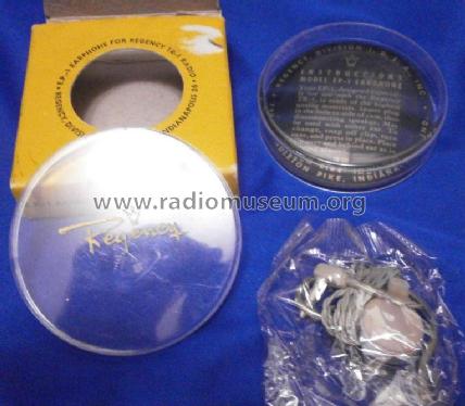
The final amplifier is operated with the emitter grounded through a 1,000 ohm resistor. Base bias is obtained from the voltage divider network formed by R13 and R14. The output transformer matches the 10,000 ohm collector impedance of V5 to the low voice coil impedance of the miniature speaker. Diameter of the speaker is only 2,75 in. Provision also exists for a small earphone plug which can be inserted into a small jack on the side of the receiver. When the earphone is in use, the speaker is disconnected.
The total power for the receiver is furnished by a hearing aid type of 22,5 volt battery. Total current drain is on the order of 4 ma.
The compactness of this receiver can be seen by an inspection of Fig. 2. All components, including the two gang tuning capacitor and the speaker, are miniaturized. Operating voltage on electrolytic capacitors, C9, C21, and C19 is 3 volts; on C17, it is 25 volts.
Dietmar Rudolph † 6.1.22, 08.Aug.12
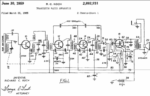
Here is a copy of the patent of Regency TR1, by Richard Koch, assigned to I.D.E.A.
Anexos
- TR1 patent part I (300 KB)
- TR1 patent part II (64 KB)
Moisés Piedade, 28.Aug.14
Dear radiofriends,
I found this announcement of the coming Regency all transistor radio in Electronics, November 1954. The article can be interesting, since it gives a list of manufacturers that developed most of the required special components.
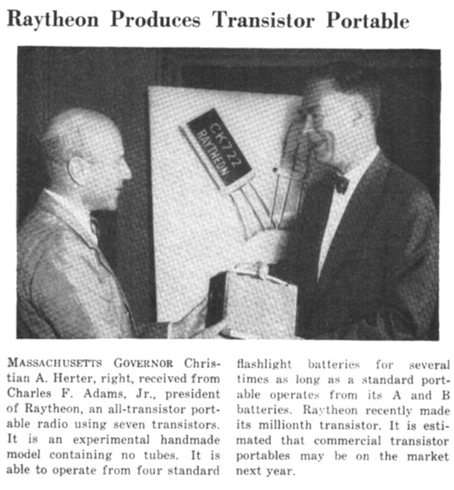
By the way, one month before, in the October issue of the same magazine, there was another announcement of a ready to come all transistor radio. Raytheon exhibited a solid state radio, an experimental prototype, given to the Massachusetts Governor.
forumdata/users/6435/file/Regency_Xradio_ad-1954.jpg
forumdata/users/6435/file/Raytheon_Xradio_proto-1954.jpg
Regards, Emilio
Emilio Ciardiello, 24.May.09
Bereits bei flüchtiger Betrachtung sah ich auf dem hochgeladenen Schema von 2006 einige Fehler; ich habe nun nicht alles kontrolliert - dazu fehlt mir die Zeit -, nur so viel:
- Das Gerät ist mit Germanium-NPN-Transistoren bestückt (also Emitter-Pfeil raus)
- der Abblockkondensator von 1nF am Collector des 4. Transistors fehlt
- die Ohrhörerbuchse ist nicht eingezeichnet
Die Germaniumdiode im Demodulator: es wurden Typen von Raytheon (CK706), Tungsol (TS117) und event. auch Typen von anderen Firmen verwendet.
Der Stromverbrauch des Gerätes liegt bei typ. 4mA (3,5 ... 4,8 mA).
MfG G.Stabe
Günther Stabe † 19.8.20, 09.Apr.07
Kurzfassung: Als „Erstes Transistor Portable“ in einer ungebrochenen Reihe zu stehen, hat sicher für viel Diskussion im Entwicklerteam unter Leitung von Richard „Dick“ Koch zusammen mit Texas Instruments, als Aufraggeber, gesorgt. TI hat damit nur 6 Jahre nach der Erfindung der Transistoren für eine Überraschung gesorgt.
Iin Wikipedia existiert ein lesenswerter Eintrag u.a. mit der Bemerkung eines „hohen“ Stromverbrauches zwischen 4 und 5 mA aus der 22,5 V Batterie. Im en.wiki ist noch die Zwischenfrequenz mit 262 kHz zu finden. Ein Zugeständnis an die damaligen Transistoren, was aber eine geringe Spiegelfrequenzunterdrückung und daraus resultierende Pfeifstörungen zur Folge hat.
Der Beitrag des Artikels von 1959 von Herrn Prof. Rudolph beschreibt die Funktion qualitativ als auch die ZF von nur 262 kHz. Im Folgenden eine versuchte Nachrechnung der Schaltung. Die für Transistorgeräte ungewöhnlich hohe Speisespannung ist vom Entwicklerteam notwendigerweise so gewählt worden. Die Streuung der Stromverstärkung auf die elektrischen Eigenschaften ist gering. Arbeitspunktstabilisierung bei absinkender Batteriespannung ist nicht vorgesehen.
Weiter im Detail:
Vorher noch eine Bemerkung zur Nachempfindung der Gedanken der Entwickler. Bei der Entwicklung von Geräten für die Massenproduktion müssen Toleranzen von Bauteilen möglichst so eingeplant werden, dass sie nicht zu großen Streuungen der Produkte führen und anderseits Berechungen mit 10 % Toleranz bei sekundären Eigenschaften zulässig sind, da die Bauteile selbst höher streuen. So wurde es zumindest bei Hornyphon gehandhabt. Das heisst natürlich nicht, dass primäre Eigenschaften, z.B. die gewählte Zwischenfrequenz oder die Bandgrenzen auch weit streuen dürfen und auf < 1kHz eingehalten wurden. Über Temperatur waren bei den Bandgrenzen einige kHz mehr zulässig. Ebenso die Junktiontemperaturen speziell bei Germanium.
Die Nachrechnung erfolgt mit einer Spannung von 20 V + ~0,15 V für das Vbe von Ge-Transistoren und zeigt was im Absatz oberhalb u.a. gemeint ist.
In Ermangelung von detaillierten Daten der Transistoren wurde auf die Daten von OC44, OC45 und OC71 zurückgegriffen.
1.NF Teil


R13 und R14 bilden einen Spannungsteiler mit einem Innenwiderstand von 3,5k und ergeben genau die Spannungswerte, die im Schaltbild eingetragen sind unter Berücksichtigung einer Streuung der Stromverstärkung von 20…70. Bei den typ. 2 mA und den nicht durchsteuerbaren Spannungsabfällen am Emitter und Transformatorwiderstand ergibt sich eine Spannung von 16,5 Vs bei 2 mA und so ein Arbeitswiderstand von ~8 kΩ. Trägt man die ~8 kΩ im Quadranten 1 ein, so erkennt man den kleinen Einfluss der Ausgangsadmittanz auf die Ausgangsleistung. Die Induktivität der Primärseite des Ausgangstransformators hängt von der gewünschten unteren Grenzfrequenz ab, die mit 400 Hz angenommen sei. Es ergeben sich 3,2 H incl. der Vormagnetisierung durch den Kollektorstrom.
Das Übersetzungsverhältnis ist dann bestimmt durch die Lautsprecherimpedanz und wird nicht weiter betrachtet.
Die unbegrenzte Ausgangsleistung ist also 17 mW. Mit etwas Klirr kann man 20 mW annehmen.
Da die NF Stufe keinerlei Gegenkopplung zeigt ist ein kleines Detail nicht ganz unwichtig: Das voll aufgedrehte Potentiometer steuert den NF-Transistor mit 1kΩ an. Die parallelen 3,5k vom Spannungsteiler sind vernachlässigt, da meist nicht mit max. Ausgangsleistung gehört wird.
Wenn man diese max. 1kΩ im 3. Quadranten des OC71 Datenblattes einzeichnet, erkennt man eine, wenn auch nur marginale Linearisierung an der Eingangskennlinie, was den Klirr nicht so groß werden lässt. Bei kleineren Lautstärken ist das ohnehin weniger wirksam. I.a. kann man sagen, dass bei einer eff. Steuerspannung von 2 mVeff = 5,6 mVpp der Klirr < 2% bleibt. Quelle 22RL673 Entwickler. Bei voller Laustärke wird eine Spannung von jedenfalls 25 mVeff an der Basis des OC71 aus dem Detektor verlangt, was auch aus dem Datenblatt des OC71 entnommen werden kann. Das gilt übrigens fast ausnahmslos für die meisten bip. Transistoren. Mit 70 mVpp lassen sich Kollektorströme etwa 1:10 verändern.
Die Eingangsimpedanz für Kleinsignalaussteuerung des NF-Teiles liegt im Bereich von 260 .... 900Ω.
Die Kleinsignalverstärkung, bei fast Spannungssteuerung = Potentiometer auf 260 Ohm, des NF-Teils liegt damit, bezogen auf den Kollektor, bei 300 …. ~600. Das ist hoch, aber auf die Speisespannung von 22,5 V zurückzuführen. Bei 6 V würde es ganz anders aussehen.
2. ZF Teil


Die Schwierigkeit liegt darin, dass die Rückwirkungskapazität und das Übersetzungsverhältnis der ZF Kreise aus den Bauteilwerten abgeschätzt werden muss. Der OC 45 hat ein Cre von 7…10…14 pF.
In Analogie dazu bei, siehe Schaltbild von 100 -200 pF im TR1 ergibt sich ein Übersetzungsverhältnis von ~1:10…1:20. Die Widerstände R6 und R9 sind zur Optimierung der Neutralisation eingefügt. Im Beitrag von Prof. Rudolph ist zu lesen, dass Texas Instruments zu jedem Transistor den Neutralisationskondensator mitgeliefert hat.
Wieder hat die hohe Speisespannung die Dimensionierung mit diesem Übersetzungsverhältnis ermöglicht. Der Detektor muss ja zur Regelung etwa 0,6V Richtspannung noch bei der unteren Speisespannungsgrenze von etwa 15V liefern können. Durchsteuerbar sind dann etwa 13,5V, was dann 1…1,35Vp an der Detektordiode, je nach Wahl des Übersetzungsverhältnisses des letzten ZF-Filters, anbietet, vermindert um den Spannungsabfall und den Durchlasswiderstand der Diode. In Radios arbeitet man üblicherweise immer im linearen Teil der Diodenaussteuerung im Gegensatz z.B. zum preisgekrönten Detektor von Prof. Bosch.
Bei einem Gerät mit einer minimalen Speisespannung von 4V müsste das Übersetzungsverhältnis etwa 1:2 sein um die AGC funktionstüchtig zu erhalten. Der im RMorg zu findende „Emperor“ mit 1,5 V Speisung ist sicher die Grenze mit ~ 1:1.
Die DC Einstellung von Transistor V3 erfolgt, ohne einen zusätzlichen Bauteil zu benötigen, vom Emitter der NF-Stufe. Es wird, wie zu erkennen, wirklich an Bauteilen gespart, wo es möglich ist.
Die Leerlaufgüte der Spulen wird mit 100 bei 262 kHz angenommen. Die Betriebsgüte darf nicht zu hoch liegen um bei 262 kHz einen noch brauchbaren NF-Frequenzgang zu erhalten. Ziel wäre z.B. eine 3 dB Bandbreite von noch 6 kHz.
Die Betriebsgüte wird bestimmt aus der Summe der Leitwerte der Leerlaufgüte selbst, dem Ausgangsleitwert des OC45 mit 15 ….40 µS, den transformierten Leitwerten der Eingangswiderstände der nächsten ZF-Stufe bzw, der Detektorschaltung. Normalerweise dimensioniert man die Betriebsgüte so, dass der Eingangswiderstand der nächsten Stufe nur einen geringen Einfluss hat.
Bei Qo = 100 ergibt sich ein Leitwert von 3,6 µS
Der Ausgangsleitwert im Bereich 15….40 µS
Der Einfluss der nächsten Stufe 1,5…10 µS bei 1:20
Die Stufenverstärkung der geregelten ZF-Stufe beträgt bei 1:20 und 1 mA etwa 50 und ist vergleichsweise sehr hoch, was aber eine gut eingestellte Neutralisation benötigt. Die letzte ZF Stufe hat dann bei nur 0,6 mA eine Verstärkung von 30 auf die Richtspannung bezogen.
Bei Nominalwerten wird der Gesamtleitwert, der stark vom Ausgangsleitwert des Transistors bestimmt wird, bei etwa 25 µS liegen, die Betriebsgüte liegt damit bei etwa 15....18, was nicht sehr hoch ist. Die Selektion wird demgemäß fast ausschließlich durch die Transistorparameter und den Widerstand R12 bestimmt. Die Bandbreite wird auch durch die geänderten Einstellungen über den Regelbereich etwas beeinflusst.
Die Gesamtselektion aller 3 Kreise wäre dann im Durchschnitt wie im nächsten Bild zu sehen.

Skala mit 5 dB / Division
Die Selektion gilt für Qb=18, Bandbreite etwa 6 kHz, S10 etwa nur 15 dB entsprechend dem amerikanischen Kanalraster. Die Werte sind nicht überragend. Es kann sein, dass die Transistorparameter für etwas bessere Selektion etwas anders sind als die des ersatzweise angenommenen OC45. Anderseits kann auch bei der Dimensionierung der Neutralisation zusätzliche Entdämpfung mit im Spiel gewesen sein. Aber diese Überlegungen sind Vermutungen, die jedoch auf Erfahrung beruhen, die z.B. im Beitrag „Ab Modell“ Minerva Minx 571 beschrieben sind.
3. Mischstufe

Der Strom in V1 variiert von 0,3 bis 1 mA, entsprechend einer Stromverstärkung im Bereich von 8,2 …~46. Den Strom nur mit R1 einzustellen ist eine eindeutige Sparmaßnahme. Die Rückkopplung des Oszillators muss entsprechend groß sein, damit auch noch bei 15 V Batterieendspannung der Oszillator noch anschwingt. Normalerweise legt man die Mischstufe für 100 mVss am Emitter aus. Damit wird der Strom 1:10 durchgesteuert, was einem „Modulationsgrad“ von fast 100% entspricht, entsprechend einer Mischverstärkung von -6 dB gegenüber der Geradeausverstärkung.
Auf Grund der Stromeinstellung von 0,3 bis 1mA streut die Verstärkung dieser Stufe um 1:3 von etwa 7….25 bezogen auf die Basis von V1. Auf den Antennenkreis bezogen eben um das Übersetzungsverhältnis der Spule am Ferritstab reduziert.
Bei 1:10 der Ferritstabspule wäre dann die Stufenverstärkung 0,7…2,5.
Die Gesamtverstärkung bei m=30% ergibt sich dann im Mittel zu
Vges= 1,5*50*26*0,3 = 585
100 µV am Antennenkreis führen zu 58 mVeff NF am Potentiometer und steuern den NF-Teil gerade voll aus, da die NF-Spannung noch durch die Eingangsimpedanz des NF-Teiles reduziert wird. Diese Empfindlichkeit des Gerätes liegt im üblichen Bereich.
Aktuelle Geräte, wo die Gesamtfunktionen in einem einzigen IC liegen, lassen solche Betrachtungen gar nicht zu. Einer meiner Entwicklungsingenieure sah seine Funktion auf ein gutes, verkopplungsfreies Layout beschränkt, da die Eigenschaften der integrierten Bauteile eben fast vorgegeben sind. Abschließend noch eine kleine Nebenbemerkung: Für die Partner Texas Instruments und die Entwicklungscrew war der Auftrag geschäftlich begründet . Für Letztere wiederum, als Erste so ein Gerät zu entwickeln, waren sicher auch Emotionen dabei. Was Vielen bekannt sein wird die als Erste ein Ziel erreichen.
Rudolf Drabek, 25.Nov.16