History of Telefunken Semiconductors
History of Telefunken Semiconductors

History of Telefunken Semiconductors
Copyright Mark P D Burgess 2012
Telefunken was created in 1903 in the dawn of commercial wireless, the high stakes era of imperial ambitions of the super powers and the development of international industrial alliances determined to exploit new electrical and wireless technologies that would prove to be vital in controlling empires and in the looming World Wars of the first half of the twentieth century.
While the superpowers exercised colonial ambitions, the giants of wireless such as Marconi, Siemens, AEG and General Electric traded, pooled, manipulated and disputed key patents with a view to creating technological monopolies that would assure massive profits.
In Germany Siemens and AEG competed for German military contracts and international business against Marconi, the dominant power in wireless at the time. At the same time Siemens and AEG were locked in patent battles both with each other and ultimately with Marconi. Realising that Germany needed one powerful wireless company, the Kaiser, Wilhelm II, ordered that the two companies pool their resources and patents through the creation of a joint venture company that would focus on the development of wireless and a dominant position internationally.
This company became known as Telefunken.
(Picture right, an early version of the Telefunken logo featuring the sparks (funken) associated with wireless of the time.)

In the pre-history of semiconductors material science, Karl Ferdinand Braun had discovered in 1874 that metal sulphides showed unidirectional conductivity. At the time Telefunken was formed, Braun was working for Siemens on crystal detectors and was one of the distinguished scientists to join Telefunken.
In 1906 Telefunken filed a patent based on his work covering an improved detector design. [Telefunken 1906] Crystal detectors were notoriously unreliable and worse, gave no amplification. By the 1920s they had been displaced by vacuum tubes but would be revisited during World War II for the detection of the ultra high frequencies developed for radar for both the Allied and Axis powers.
Picture: the Braun detector design from Telefunken 1906
Telefunken Radar Detectors
The importance of radar to the Allied war effort and the development programme led by the Radiation Laboratory of MIT is well documented. [For example, Torrey 1948, Seitz 1998] The development of the cavity magnetron in Britain and the potential for high resolution radar led to a large scale development programme managed by the Radiation Laboratory at MIT. This included the development of new crystal rectifiers: a redeployment of very old technology now revisited because vacuum tubes could not operate at the GHz frequencies being used. But to meet military standards the vintage crystal detector needed to become a reliable detector.
In Germany radar research was not prioritized until a British Stirling bomber was shot down over occupied Netherlands south of Rotterdam in February 1943. Its H2S ground mapping radar was recovered and sent to Telefunken for evaluation. Its significance was quickly understood and a committee named after the crash location (Arbeitsgemeinschaft Rotterdam) was set up to recommend countermeasures.
When Germany discovered how far it had lagged the Allied developments it urgently assembled teams of over 1000 scientists and engineers needed for its own radar programme. The Telefunken team was led by Horst Rothe and included theoretical physicist Karl Seiler, Herbert Mataré and the physical chemist Paul Ludwig Günther to design Silicon detectors. [Handel 1998]
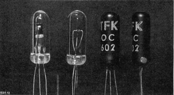
Telefunken ED Series Silicon Detectors
Telefunken worked on silicon detectors while Siemens developed germanium detectors. Silicon detectors were found to be more suited to short wavelengths because they had a better recovery time.
Crude silicon was readily available but difficult to purify due to its very high melting point and high reactivity. It was used in early detectors but did not give reliable performance. Progress was made when Karl Seiler collaborated with Paul Ludwig Günther a physical chemist working at Breslau for the Reich Aviation Ministry. Günther had been working on synthetic metal sulphides such as pyrites that had been used in their natural form as detectors in the early days of wireless.
Making pure synthetic pyrites had proved too difficult so Günther had moved on to another traditional detector: Silicon, used since the wireless days by Telefunken. Picture right: an ED149 silicon detector from 1919 [Telkefunken 1919]
Günther developed a method of producing improved silicon by reduction of silicon tetrachloride and used this approach to deposit layers of silicon on ceramic substrates. This could be done at 800C, well below the 1440C melting point of silicon. To make a detector silicon needed to be deposited onto a conductor and Telefunken first tried molybdenum unsuccessfully (the silicon flaked off) and then graphite which proved satisfactory.
The silicon was produced using aluminum as the reducing agent and this was a lucky choice: Aluminium contaminated the silicon creating P-type silicon. Interestingly, in Britain, GEC were making “red spot” silicon detectors that were also aluminium doped.
While Seiler and Günther worked on silicon layers at Breslau, Mataré worked at Leubus investigating different types of detectors.

Pictures of the ED701 and ED702 courtesy of Joe Knight showing a relatively crude state of development and a single point contact design later abandoned.
Reliable designs were completed by December 1943 for the Telefunken ED700-ED705 range of detectors for centimetre wavelengths. (Note Telefunken continued the use of the “ED” series initiated in the days of wireless.) By April the following year the new synthetic silicon detectors were in service. They were used in the Naxos radar detector and the Berlin radar used by the Luftwaffe night fighters to find the location of raiding bombers.
In production silicon was deposited onto 1.4mm graphite rods which were broken and soldered into a brass cap creating an ohmic connection to the graphite. The rectifying contact was made from a molybdenum wire loop which pressed against the silicon coating. The loop was fixed to a grub screw which could be adjusted.
Use of a loop contact offered good vibration resistant stability but caused more noise. And compared to a point contact design, higher capacitance and inductance which degraded high frequency performance. [Handel 1999] The type ED705 was the final detector in the series and was introduced in October 1944 for use in the Berlin radar.
The picture below shows a WW2 vintage ED705 detector and the certificate advises that any faulty units should be returned to Telefunken at Zehlendorf, Berlin (an important Telefunken R&D and production centre which was closed on occupation). The detectors were tested for reverse and forward current and at cm wavelengths after aging as indicated on the test certificate.

Left: Diagram from Seiler K Detektorenp283; 1948 cited in Handel 1999 and translated. Right Picture of ED705 and test certificate is a reproduction as the original cannot be reproduced for copyright reasons.)
The ED705 and the ED704 shown below were the last in the line of Telefunken detectors superseding the ED700 and ED702.

Wehrmacht ED704 Detectors courtesy Andrew Wylie
The note that accompanies the ED704 advises that the types ED704 and ED705 can replace ED700 and ED702 provided the correct adapters are employed. Note: while these detectors are unbranded they are known to be Wehrmacht origin having been abandoned after the surrender of the German forces in Norway in 1945.
Telefunken and Mataré’s work at Leubus had to be abandoned as the Soviet army advanced against Leubus in 1944 causing the laboratory to be evacuated.
Detector Noise
A feature of point contact detectors was high noise and Telefunken engineers, including Mataré had significant expertise in noise measurement. Mataré worked on balanced duo-detector circuits which would have a self cancelling noise characteristic provided the detector pair were accurately matched. To obtained matched detectors Mataré experimented with two point contacts closely aligned on a crystal surface. (Diagram right of push-pull detector circuit from Mataré 1951 as reproduced in Handel 1999.)
”Early on, the director of research, Horst Rothe, gave us the task of comparing electronic noise measurements for vacuum mixer diodes and crystal rectifiers. We also studied the compensation of the oscillator noise through the use of duodiodes in push/pull microwave mixers and the improvement of the signal/noise ratio through the use of crystal mixers with crystals such as silicon, silicon carbide, lead sulfide and germanium. And we sought ways to equalize the current/voltage characteristics of crystal duodiodes for oscillator noise compensation.
In fact, I made three-electrode crystals, trying to locate both top whiskers so that the current/voltage characteristics were identical. But the crystal material was so inhomogeneous that most tests failed to result in noise compensation. In 1942, though, we published our results on noise measurements in crystal rectifiers.
The following year, I applied for a patent on crystal diodes with electrolytic contacts, and later I sought one on crystal duodiodes for centimeter-wavelength mixers. Eventually, better crystal material became available. Karl Seiler of Breslau University evaporated silicon on graphite substrates and Heinrich Welker of the Institute of Physical Chemistry in Munich used the Bridgman technique to make germanium crystals.” [Mataré 1998]
The arrangement of two point contacts closely aligned on a crystal that Mataré employed was potentially a point-contact transistor and some unexplained effects were observed: “I found during some tests that I got interference from one characteristic on the other, but I had no time to study this further because of production pressure to deliver the duo diodes and also due to abandoning the lab in 1944 when the Soviet army occupied Silesia.”[Mataré 2002]
![]()
Four years later when working at the Société des Freins et Signaux Westinghouse,France, Mataré and his German colleague, Heinrich Welker who had worked at University of Munich during the war on germanium detectors supporting the Siemens’ programme became well known for their post war work on the first European transistor, the Transistron. (Picture of 1948 prototype Transistron courtesy Deutsches Museum Munich and the BBC.)
ED Detector Production in the GDR After 1945
Following the end of World War II Germany was partitioned into countries: The German Democratic Republic (GDR) aligned with the Eastern European bloc (East Germany) and the Federal Republic of Germany (FDR) aligned with the West (West Germany). The re-unification of Germany occurred 45 years later in 1990.
As a result of the war Telefunken factories were destroyed and many of its scientists scattered or sent abroad under the direction of the occupying forces in order to strengthen their home economies. However, on both sides of the divided nation, work began immediately rebuilding research and production facilities. The associated politics reflected the Cold War and the competing technologies of both sides created a great deal of military intelligence including now declassified reports by the CIA.
After the capitulation of Berlin in May 1945 to the Soviet forces, the Soviets established LKVO, a research and development laboratory at the AEG tube factory at Oberschöneweide. Its first manager was Karl Steimel, a Telefunken tube designer. LKVO effectively continued the business of AEG and its associate company Telefunken in the GDR.
In 1946 LKVO was amalgamated with Nachrichtentechnische, Entwicklung und Fabrikation and the new organization was known as OSW. It was directly run and controlled by Soviet authorities and known as anSAG (Sovietische Aktiengesellschaft).Employing 2000 scientists, engineers and workers, it was intended the research institute would supply developments to enhance Soviet production. By 1947 there were seven departments and 22 divisions covering all electronics and materials research. In January 1951 the organization was renamed HF and in 1960 WF, as summarised in the following table.(Logos and history courtesy Schmidt 2011.)

After the war Telefunken diodes were produced by OSW. In 1947 approximately 5000 ED704, ED705 and ED707 detectors were produced and this was probably the last year of their production.
According to the CIA report “At least three types of crystal detectors have been mentioned, the ED 704,705 and 707. Research is in progress on the growing of silicon monocrystals on carbon rods for use as detector crystals. So far is not been possible to form the crystals sufficiently firmly on the carbon.
In the present detectors, silicon is condensed from silicon tetrachloride in both ends of the carbon rods at a temperature of 800C. These are then bisected and used in the detector tubes 704 etc, No detectors for 4mm waves are being manufactured; the lowest wavelength attained is 8mm.” [CIA Report 1949]
 Some ED704 were branded WBNwhich was the logo of Werk für Bauelemente der Nachrichtentechnik founded in 1949. (Picture courtesy Joe Knight)
WBN was associated with the Forschungsinstitut für Halbleitertechnik (IHT) founded by Professor Matthias Falter at Teltow and has been described by Salomon as the “cradle of the East German semiconductor industry.” It appears to be linked with the crystal detector work done by AEG and OSW at Oberschöneweide, Berlin. [Salomon 2003]
 The close similarity is not in itself evidence of linkage given they needed to be interchangeable replacement parts.
For example, radar detectors were also produced in the USA in standardized formats.
Picture left: two radar detectors by WF and WBN. Courtesy Joe Knight
Telefunken Semiconductor Research
Following the end of the war Telefunken built a tube plant at Ulm. Horst Rothe was the director of  development having been director of the war time Telefunken detector development. (Picture of Horst Rothe from Handel 1999 citing Rukop 1952)
Telefunken obtained a license to the Bell Laboratories transistor patent estate and accordingly was entitled to attend the 1952 Bell Licensees Symposium where attendees were introduced to the point-contact and grown junction transistors as well as many of the key process technologies for their manufacture.
The other German licensees were Siemens & Halske and Felten & Guilleaume. [Lojek 2007] New companies were established such as Proton founded by Wolfgang Büll in Planegg near Munich, Kristalloden, the firm of Rudolf Rost and Intermetall, founded by Herbert Mataré and investor Jakob Michael in 1952.
In Germany the first company to produce a transistor was Rudolph Rost’s company, Kristalloden in Hannover which launched a range of point-contact transistors in 1952 (GT10 GT20 GT30). Later in the same year, Süddeutsche Apparate-Fabrik (SAF) an associate of Felten & Guilleaume introduced the VS200 point contact transistor. [Herzog 2001] Proton had a germanium diode also by 1952 based on the wartime work of Henrich Welker. [Adam 2011]
At Ulm Telefunken had established a small research unit to develop semiconductors. Key persons were:
Dr J Malsch, Director of Semiconductor R&D
F W Dehmelt and W Engbert, Beneking, Heinz
In addition to knowhow from Bell, Telefunken had a no-compete agreement for Germany with RCA as part of a patent pooling arrangement. [Mirow 1982] RCA licensed Telefunken its semiconductor technology and exchanged information on improvements with them through its technical bulletins. [Flaningam 1945 Herold 1953]
Point-Contact Diodes
Telefunken’s first products were glass encapsulated germanium diodes. The pictures below show part of the manufacturing process. On the left, an unsealed diode is aligned with the help of an oscilloscope. Once the desired characteristic is confirmed, the diode is sealed into a glass enclosure using micro gas torches to fuse the glass around the leads.
By 1953 Telefunken had six plants and five offices in Berlin, Ulm, Frankfurt/Main and Hanover producing a very wide range of electronics for broadcasting, commercial and marine applications. In 1953 Edward Herold, who was responsible for the RCA semiconductor programme, made a tour to Europe to visit the company’s European licensees. He met Telefunken in October 1953 and reported that Telefunken had commercial diodes in production and that two types were in production: “ordinary” types based on 5 ohm-cm germanium and video types using 0.5 ohm-cm germanium. The diodes were sealed in glass using dumet leads and a tungsten point-contact. The line had a small automatic sealing machine operating at 50 per hour.

Diode assembly: Left alignment, and Right, fusing the diode in a glass enclosure [Rost 1956]

Early Style Telefunken Diode courtesy Radio Museum
|
Part of a datasheet for Telefunken Diodes C1955 |
Telefunken were producing high purity germanium using a variation of the Czochralski technique. This employed a double carbon crucible designed to maintain constant doping of the pulled crystal by bleeding high purity germanium into the inner crucible to compensate the otherwise increasing concentration of the dopants. Picture: under vacuum a single crystal of germanium is pulled from a melt. [Rost 1956] |


Point-Contact Transistors
Some work was being done on point-contact transistors including the use of resin or a glass-dumet seal developed for their point-contact diodes using tungsten or vanadium steel for the emitter contact.


Photos of experimental crudely resin encapsulated Telefunken point contact transistors
courtesy of Rudi Herzog.

Photo of a glass sealed Telefunken point contact device courtesy Rudi Herzog
In addition Telefunken developed more sophisticated point contact devices. The first Telefunken transistor exhibited in 1953 was an experimental type GC1 and obviously made only for demonstration purposes having clear glass encapsulation. The area of the junction has been protected in resin. The Telefunken GC1 is a very unusual point-contact transistor featuring gold whiskers.
The collector lead was antimony doped gold (N-type) and the emitter lead gallium doped gold (P-type). A Telefunken DF651 subminiature pentode bulb was adapted for use as the transistor header and envelope. Further information
|
Telefunken GC1 courtesy Siegfried Neumann and Radiomuseum |
The wrapper states that the collector whisker is 0.15mm antimony doped gold (N-type) and the emitter whisker gallium doped gold (P-type).
|


Grown Junction Transistors
As was the case with most companies at that time Telefunken worked on grown junction transistors.
In 1955 Malsch described this and the rate growing process developed by Robert Hall [Hall 1952] which Malsch calls the “zone growth” process in which NPN structures could be obtained by exploiting the fact that in a melt that contained both N and P type impurities, the incorporation of antimony (N type) is strongly dependent on crystallization rate: more is incorporated at high growth rates creating an N type layer whereas a P type layer could be created by slowing crystal growth.

A zone growth crystal with its characteristic profile due to the cycling of growth rates
The profile enabled the crystal to be easily cut up into slices so that each disc contains three zones forming the transistor. From the individual slices transistors were then cut-out. A special etching process made the pn junctions visible and easy to accurately locate. The main difficulty in the completion of these transistors was making a connection to the base so that the junction was not shorted.
These processes were hard to control, Malsch noting: “One can also readily imagine that in this zone growth method, it is not easy to maintain precise control of the necessary conditions for mass production. Even during the pulling of a crystal the consecutive layers are different, because the concentration of the melt changes continuously.” Alloy junction transistors quickly became the dominant technology. “The zone growth method is history and plays only a relatively minor role in today’s production. But we have the impression that it has a great future for high frequency transistors.” [Malsch 1955]
In 1953 Telefunken also had alloy processes and had a power rectifier in development using a 12 mil wafer of high conductivity germanium alloyed with commercial grade indium. And work was underway on an alloy junction transistor including the development of a metal hermetic seal thought to be needed to avoid high temperature glass seals
Production Transistors
The German industry used the Industrial Fair at Hannover to announce their new devices. Whereas up until 1953 only point-contact types had been exhibited by Kristalloden, Siemens, SAF and Intermetall, 1954 was the year of the alloy junction transistor. Telefunken announced its Alloy PNP types OC601 and OC602 for low power audio frequency applications.

New Telefunken Types OC601 and OC602
Above: the new transistors shown as advertised in journals of the day compared to a 10 pfennig stamp featuring President Heuss. These transistors were encapsulated in silicon grease which fills the glass envelope. The seal between the glass envelope and stem was closed with epoxy resin. [Johnson 1954] By 1955 Telefunken had adopted a narrow cylindrical profile.
Alloy Junction Transistor Production
In 1955 Director Malsch described how Telefunken were making alloy junction transistors giving examples of their power transistors and the OC602. [Malsch 1955] These were conventional processes used at this time.
|
Zone purification of germanium indicating seven melt zones. High purity (almost intrinsic) germanium is cut from the formed crystal and placed in a graphite crucible and transferred to the crystal puller. |
|

|
Close-up of the crystal puller which operates under vacuum to protect the germanium from oxidation. Picture shows a crystal being pulled from a seed crystal. The melt contains either N type or P type impurities at carefully controlled levels |
|


|
Single crystal and seed. During pulling care is taken to ensure that the crystal orientation is controlled. eg in the 1-1-1 direction or the 1-0-0 direction. |
|

|
Next the crystal is sliced into thin sections and then cut into rectangular tiles whose dimensions depend on the desired performance of the transistor |
|

|
Germanium rectangular slices are carefully sanded, polished and etched and then alloyed with indium dots on either side. (Picture shows power transistor alloyed slices.) |
|

|
The transistor is attached to the header by welding its wires. (Glass type is illustrated) |
|

|
Completed OC602 transistors: unpainted and painted (to avoid exposure to light). Note that by 1955 Telefunken had adopted its familiar small cylindrical profile. |
|
At the April Hanover fair of 1955 Telefunken showed its new OC603 (low noise) and OC604 both for low power uses. Later in the year the medium power OD604 was introduced.
In approximately 1955-56 Telefunken produced a data book of its tubes and transistors for English speaking countries.
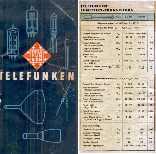
This link will take you to a composite of the front cover of the data book and the page giving data for the OC601 and the OC602.
Telefunken TR1 Prototype Radio
It seems possible that an early prototype of the TR1 was shown privately at the 1955 Hanover fair. [Gebert 1997]
Later that year, Telefunken made approximately 100 pre-production six transistor radios for release to the trade for evaluation at the 1956 Hanover fair. The TR1 is considered to be the pre-production version of the Partner that was launched in 1957. (Picture of the TR1 from Schlegel 1956)
At this time Telefunken had no RF transistors but in the tradition of the times, was able to select suitable OC602 transistors from production that would serve in the first five RF and IF stages. A low IF frequency of 270 KHz was selected to facilitate better stage gain. Neutralisation was necessary to offset the effects of internal feedback and parasitic oscillations due to the high base-collector capacity of these transistors.
The six stages were:
Oscillator
Mixer
Intermediate Frequency stages (3)
A single class A audio frequency stage using the new OC604 was used to drive a speaker.
The Telefunken TR1 came out a year after Regency launched its TR1 developed in collaboration with Texas Instruments. TR is a common designation given to Telefunken equipment and the similarity of the names is a coincidence. But there are design similarities including the IF neutralization, the high battery voltage of 22.5V and the use of a Jensen speaker. A more detailed comparison of the two designs can be found in Gebert 1997.

Telefunken TR1 from Rost 1956
New RF Transistors and the Partner 1
With the advent of the development of high frequency transistors manufacturers rushed to develop  designs that would exploit the new IF transistors and RF transistors in an all transistor portable radio.
The IF stage OC612 designed for the conventional IF frequency of 470KHz and was introduced in the fall of 1956.
At the Hanover Fair of May 1957 Telefunken launched their first RF transistor, the OC613 which had been narrowly preceded by the Valvo OC44. Both were designed for MW oscillator/mixer duty. Picture left: an OC612 and OC613 courtesy Andrew Wylie.
These transistors were used in the first German pocket radios: The Peggie from Akkord and the Partner 1 from Telefunken.
The Telefunken Partner used the new OC613 in its front end, two OC612 in its IF stages and two stages of AF amplification using a OC604 and a single OC604 spez output. [Radiomuseum Accession 4024]

Partner 1: First Commercial Telefunken Transistor Portable
The Partner was an elegant design with a significant drawback: limited production of the new Telefunken transistors restricted availability. The Partner featured printed circuits, ferrite aerials and miniature components suited to the compact designs. The IF stages required careful neutralization to prevent spurious oscillations due to the high inter-electrode capacity of the IF transistors.

The circuit board for the Partner 1 [Toute la Radio July 1957]
The set that stole the show was the Peggie from Akkord which was designed around the same five 
 transistor set as the Partner but went to market using an alternative set from Valvo: OC44, two OC45, OC71 and OC72 which were more readily available. The set was featured ahead of the Hanover Fair in Radio Mentor No 4 for April 1957. [Radiomuseum Accession 356] Picture from Toute la Radio July 1957.
A relatively rare Telefunken transistor, the OC611, is believed to be an RF type although details of its intended use are sketchy. It was clearly a special purpose type that quickly became obsolete. Photo courtesy of Siegfried Neumann.
|
Summary of Early Telefunken Transistors In common with other manufacturers, Telefunken used the Hanover Electronics Fair to release many of their new transistors and reports from the Fair give a good indication of the release date of new transistors. The Fair was held at the end of April or early May each year.
|
||
|
Date |
Telefunken Type |
Reference |
|
1954 Hanover Fair |
OC601 (AF small power uses) OC602 (AF small power uses) |
1 1 |
|
1955 Hanover Fair
|
OC603 (AF low noise pre-amplifier) OC604 (AF small power uses) |
1 1 |
|
Fall of 1955 |
OD604 (medium power) |
1,4 |
|
Fall of 1956 |
OC612 (IF amplifier 470 KHz) |
1,5 |
|
December 1956 |
OC604 Spez (Class A output 100mW with cooling fin Class B 400mw) |
5 |
|
1957 Hanover Fair |
OC613 (MW oscillator mixer) OD605 (AF amplifier 15 W) |
1 1 |
|
March 1958 edition of Telefunken-Zeitung |
OC622-OC624 (Miniature AF for hearing aids) OD603 (Medium power) OC615 (FM Receivers) |
2 |
|
1959 Hanover Fair |
OC614 (FM IF amplifier) OC615 (FM oscillator mixer) |
3 3 |
|
References (1) Herzog 2001 (2) Radiomuseum (3) Toute la Radio 1959 (4) Rost 1956 (5) Telefunken 1956). |
||
Spezial Audio Frequency Types
Telefunken made "Spez" versions of some of its transistors in a long version (20mm) of its standard glass encapsulation (15mm). Inside is a conventional alloy junction structure with a cylindrical heat sink attached to the wafer carrier plate which would improve heat transfer through the glass capsule.


Left to Right: OC602, OC602 Spez with paint removed, OC602 Spez and late OC604 Spez Type
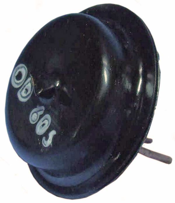
First Power Transistors
The first Telefunken power transistor was the OD604 introduced late in 1955. It was a germanium PNP junction transistor in an unusual axial design and in its most rare form, was sold without its customary metal cube heat sink.
It is normally found with a two piece metal clamp intended to improve heat transfer. This transistor could handle a maximum collector current of 2 amps and a maximum collector dissipation of 1.3 watts.


Left: the OD604 and Right: OD604 in its heatsink mounting. (Photo courtesy Andrew Wylie.)
This transistor is not found in many devices: It was usually used in Class B push pull audio output stages with up to 4 watts output. Radiomuseum notes that only three devices used this transistor:
The 1957 Akkord Trifels hybrid tube/transistor AM/FM portable radio with a five transistor audio amplifier using OC602, OC602, OC604spez and two OD604 in a class B output. (This set also uses a transistor DC/DC converter for the tube HT supply using a GFT32.)
A 1957 Gigafon T megaphone employing a six transistor audio amplifier using two OD604 in a class B output.
A 1958 Telefunken: ELA V630 4 Watt battery powered audio amplifier with seven transistors using two OD604 in a class B output.

OD605
The OD605 was developed and released in time for the Hanover Fair of 1957. It was the heavyweight of the range developed in the 1950s with a collector dissipation of 15 watts and a collector current of up
 to 10 Amps. [Herzog 2001]
Picture courtesy of Siegfried Neumann and Radiomuseum.
OD603
 In March 1958 Telefunken-Zeitung, the in-house Telefunken technical journal, covered the first of a new higher performance power transistor, the OD603. In this design the collector dot was soldered directly
 to the transistor header.
 The transistor was sealed into its enclosure under dry air which also improved heat transfer. A separate mounting flange was available to secure the transistor firmly to a heat sink such as a metal chassis and electrical isolation was assured through the use of a mica insulator.

These design elements enabled a maximum 4 Watts dissipation. Picture, right courtesy of Siegfried Neumann and Radiomuseum.
Cross Section of an OD603 from Telefunken 1960
Early applications for this transistor were in a 1958 Blaupunkt hybrid automobile radio where the transistors were used in a class B audio output stage and in 1959 in two Telefunken all transistor audio amplifiers where these transistors were also used in the output stages.


These pictures (courtesy of Bob McGarrah) show the mounting kit for the OD603 (above left) and right, an inside view of the transistor. The germanium wafer is obscured by the base plate which provides the base connection. The emitter connection is via a hole in the base plate and the collector dot is soldered directly to the transistor header as shown in the diagram above.
Transistor Range Early in 1958
A view of the Telefunken range is given in the following advertisement from a 1958 databook as at the beginning of 1958.


From the back cover of Kristalldioden und Transistoren Taschen Tabelle, 2nd edition, published by Franzis-Verlag München.
Improved Transistor Construction
By around 1960 the relatively crude outline and structure shown in Malsch in 1955 had been streamlined by improved production technology. Telefunken continued to use glass enclosures but the assembly of the transistor elements was more mechanised.


Internal Structure of a OC603 courtesy Ulf Seifert aligned with a schematic from Telefunken 1960
The collector and emitter dots were stamped out from indium strip metal. The germanium wafer was soldered to a nickel base plate using a solder perform. The emitter dot was alloyed to the underside of the transistor assembly through a hole in the base plate. [Telefunken 1960]
High Performance RF Transistors

![]()
The first strategy for improved high frequency performance was to reduce the dimensions of the standard alloy junction transistor. In the above diagram the size of a small signal audio frequency type is shown compared to a AF101 RF type (right) designed for standard broadcast band mixer or IF stages. (the AF101 superceded the OC613.) [Picture from Telefunken 1962]
Drift Transistors
 However, transistors needed to support a FM receiver required devices that could operate in the range 87.5-100 MHz and this required new designs. The early options on high frequency performance included:
 Rate grown transistors developed by General Electric;
Surface barrier transistors developed by Philco; and
Drift transistors conceived by Dr Herbert Krömer in Darmstadt Germany
Krömer graduated PhD in 1951 and began work in the telecommunications laboratory of the German Postal Service. Initially he worked on how transistor junctions were formed in the alloy process. Much later Krömer was awarded a Nobel Prize for his work in semiconductor hetero-structures and in his Nobel Prize lecture recalled his conception of the drift transistor in 1953:
“The early bipolar junction transistors were far too slow for practical applications in telecommunications and I set myself the task of understanding the frequency limitations theoretically – and what to do about them. One approach - not the only one - was to speed up the flow of the minority carriers from the emitter to the collector by incorporating an electric field into the base region. This could be done by using, not a uniform doping in the base, but one that decreased exponentially from the emitter end to the collector end – the so-called drift transistor.” [Krömer 2000]
A year later Krömer left Germany for a research role at the RCA Princeton Laboratories. The first RCA drift transistor, the 2N247 was launched in 1956. Telefunken launched their drift transistors in 1958. Late in 1957 Kroemer returned to head the Philips semiconductor group at Hamburg and therefore ![]() there is no indication he directly
there is no indication he directly  influenced the Telefunken developments. But Telefunken did have a license to RCA transistor technology.
Drift transistors were conventional PNP alloy junction transistors where the doping of n-type impurities of the germanium wafer was high on the emitter side and very low on the collector side.
Picture of a Telefunken drift transistor showing that the n-doping is concentrated on the emitter side [Telefunken 1962]
Making a Drift TransistorA drift transistor was a conventional alloy junction transistor but made from a specially diffused germanium wafer that was high in n-type impurities on the emitter side and had very low doping on the collector side. High purity germanium was firstly diced into wafers which were then, for example, doped in an atmosphere of arsenic at a pressure of 10-3 mm Hg at 785°C. This produced a wafer that had high levels of arsenic on each surface. The side that was to become the collector side was then etched away.
Micro-alloy drift transistors were made in a similar manner but in this case a depression was etched into the collector side which would become the site of the collector.
Typical donor density in the base region ranged from 1018 to 1013 atoms per cc (from emitter to collector).
Once the base wafer was prepared the emitter and collector were alloyed in the conventional manner. [Telefunken 1962] The resulting structure conferred two further advantages in addition to the accelerating base field. Drift transistors had lower input impedance due to the higher conductivity of the base at the emitter junction and the collector capacity was reduced by the low conductivity of the base at the collector junction. Thus three factors worked together to improve high frequency performance. |


View of a OC615V Drift Transistor showing the alloy junctions and the germanium wafer mounted on the collector side. Access to the emitter junction is via a hole in the carrier plate.
Drift Transistors for Short Wave and FM Bands

 The PNP transistors that would be announced by Telefunken in March 1958 in Telefunken-Zeitung included the AF105, OC614 and the OC615 series initially in three forms:
OC614 SW mixer stages
OC615
OC615V FM pre-amplifier (FM-Vorstufe)
OC615M FM mixer (FM-Mischer)
In addition some manufacturers identified these transistors with spots on the top of the enclosure that identified the intended use. (Picture above showing the OC615 alongside its AM predecessors. Courtesy Andrew Wylie.)
The new OC614 and OC615 transistors were readily adopted to produce new portable radios in “substantial” number of models according to a report carried by Frequenz of the 1959 Hanover Fair. [Taeger 1959 ]
Acknowledgements
While all references are acknowledged below special thanks are due to the pioneering work by Rudi Herzog who published the first history of Telefunken transistors and kindly produced superb new images for this article. Joe Knight also provided material from his extensive collection of semiconductors. The author is grateful for the permission of other collectors and historians for access to their material including Jack Ward, Andrew Wylie, Ulf Seifert, Bob McGarrah, Siegfried Neumann, Peter Salomon, Christian Adam, Kai Handel and Wolfgang Gebert.
The extensive archives of Radio Museum and its members have been invaluable.
The author would be grateful for any further information and may be contacted by email: markpdburgess@gmail.com
References
Adam C 2011 The First Germanium Semiconductors: CFS Westinghouse Westectal Diodes and the Westrel Transistron
CIA Report 1949 Vacuum Tube Development at the Oberspreewerke and its Significance to Soviet Electronics Developments NND 961020-183
Flaningam M 1945 International Cooperation and Control in the Electrical Industry: The General Electric Company and Germany Am Jnl Economics and Sociology 5 No 1 7-15
Gebert W 1997 Anmerkungen zu den Schaltungen der ersten Transistorradios Funkgeschichte 115 (1997) 241-44
Hall R 1952 P-N Junctions Produced by Growth Rate Variation Phys Rev 88 139
Handel K 1998 The Uses and Limits of Theory: From Radar Research to the Invention of the Transistor Proc History of Science Society October, 1998
Handel K 1999 Anfänge der Halbleiterforschung und –entwicklung PhD dissertation available at Scribd.com
Herold 1953 Herold’s German Visits, Tubes and Semiconductors, 1953 RCA Technical Report PEM 373
Herzog R 2001 The Early History of Transistors in Germanyat the Semiconductor Museum
Johnson H 1954 Telefunken Transistors 1954 RCA Technical Report PEM502
Krömer H 2000 Quasi-Electric Fields and Band Offsets: Teaching Electrons New Tricks Nobel Lecture
Lojek B 2007 History of Semiconductor Engineering Springer
Malsch J 1955 Transistoren und ihre FertigungETZ Elektrotechnische Zeitschrift 21st August 1955 issue 8 273-278 Digital copy courtesy Radiomuseum
Mataré H 1951 Empfangsprobleme im Ultrahochfrequenzgebiet Oldenbourg, München 1951
Mataré H 1998 Breakthroughs Recalled on Transistor Precursors in Germany, France, Physics Today, 51 2 97–98
Mataré H 2002 Letter to Armand van Dormael 3/7/2002
Mirow K R and Mauerer H 1982 Webs of Power International Cartels and the World Economy Boston: Houghton Mifflin Company
Radiomuseum 4020 Partner-Vorserie TR1
Rost R Ernst H M 1956 : Kristalloden-Technik 2. Aufl. Berlin, Ernst Verlag, 1956.
Rukop H 1928 Die Telefunkenröhren und ihre Geschicht Festschrift 25 Jahre Telefunken 1903-1928 114-154
Rukop 1952 H Rothe Telefunken G.m.b.H. CIOS-Report XXXI-52; and Organization of Telefunken CIOS-Report XXI-1.
Salomon P 2003 Die Geschichte der Mikroelektonik – Halbleiterindustrie der DDR Funk Verlag Bernhard Hein e.K.
Salomon P 2006 Deutsche Halbleiter-Technik vor dem Urknall?
Schlegel H 1956 Der Transistor-Taschen-Super Telefunken TR1 Funkschau 5 1956 174-7
Schmidt H T 2011 Die historische Entwicklung des Oberspreewerkes
Seiler, K. : Detektoren Naturforsch und Medizin in Deutschland 1939-1946 Weinheim Verlag Chemie 15 272-292
Seitz F and Einspruch N 1998 Electronic genie: the tangled history of silicon University of Illinois Press
Taeger W 1959 Bericht von der Deutschen Industriemesse in Hannover 1959 Frequenz 13 Issue 6, 183–90
Telefunken 1906 Patent DE178871 Wellenempfindliche Kontaktstelle Filed 18 Feruary 1906 Granted 22 October 1906
Telefunken 1919 Zusammensstellung der modensten tönenden und ungedämpften Radio-Stationen und Geräte Der Telefunken Anfang 1919
Telefunken 1956 brochure Röhren-Dokumente Nr 3 (supplement in Funkschau 24 December 1956).
Telefunken 1960 Der Transistor Telefunken GMBH Ulm and Donau 1960
Telefunken 1962 Der Transistor II Frequenzbereich 100KHz...100MHz Telefunken GMBH Ulm and Donau 1962
Torrey H Whitmer C 1948 Crystal Rectifiers 15 MIT Radiation Laboratory Series. McGraw-Hill, New York, 1948
Toute la radio 1959 Foire de Hanovre 238 344-347
To thank the Author because you find the post helpful or well done.